Method of adopting MOCVD technology to manufacture near ultraviolet LED possessing step-type quantum well structure

A near-ultraviolet and quantum well technology, applied in chemical instruments and methods, crystal growth, electrical components, etc., can solve the problem that the output power is only the input power, and achieve the effects of improving crystal quality, increasing luminous efficiency, and relieving stress

Active Publication Date: 2016-10-19
SINO NITRIDE SEMICON
View PDF4 Cites 11 Cited by
  • Summary
  • Abstract
  • Description
  • Claims
  • Application Information

AI Technical Summary

Problems solved by technology

The photoelectric conversion efficiency of ultraviolet LEDs with a wavelength above 385nm is signif

Method used


Image

  • Method of adopting MOCVD technology to manufacture near ultraviolet LED possessing step-type quantum well structure
  • Method of adopting MOCVD technology to manufacture near ultraviolet LED possessing step-type quantum well structure

Examples


Embodiment Construction

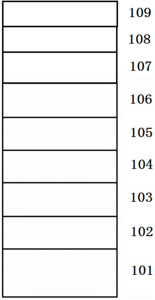
[0019] The invention provides a method for preparing a near ultraviolet LED with a stepped quantum well structure by using MOCVD technology. By designing a new type of LED structure, a stepped quantum well structure is adopted. Effectively alleviate the stress on the quantum well, improve the quality of the quantum well crystal, and improve the luminous efficiency of the near-ultraviolet LED. figure 1 It is an embodiment of the present invention, a vertical cross-sectional view of a near-ultraviolet LED with a stepped quantum well structure prepared by using MOCVD technology.

[0020] Such as figure 1 Shown is an embodiment of the present invention, a vertical cross-sectional view of a high-brightness near-ultraviolet LED with a stepped quantum well structure prepared by using MOCVD technology.

[0021] Use Aixtron company, close-coupled vertical reaction chamber MOCVD growth system. During the growth process, trimethylgallium (TMGa), trimethylindium (TMIn), and trimethylaluminum ...


PUM


Abstract

The method provides a method of adopting a MOCVD technology to manufacture a high-brightness near ultraviolet LED possessing a step-type quantum well structure. The invention discloses the high-brightness near ultraviolet LED with a peak value wavelength scope of 395-410nm. An epitaxial structure successively comprises a graphical sapphire substrate, a low-temperature GaN nucleating layer, a high-temperature non-doped GaN buffer layer, an n-type GaN layer, an n-type Inx1Ga1-x1N/Aly1Ga1-y1N superlattice stress releasing layer, an InxGa1-xN/GaN/AlyGa1-yN multi-quantum-well active layer, a p-type Aly2Ga1-y2N/GaN superlattice electronic barrier layer, a high-temperature p-type GaN layer and a p-type InGaN contact layer from bottom to top. The active-layer multi-quantum well adopts an InxGa1-xN/gaN/AlyGa1-yN step type structure. A thickness scope of an InxGa1-xN well layer is 2-4nm. A GaN stress regulation and control layer thickness is 0.5-5nm. An AlGaN barrier layer thickness is 8-20nm. Through design an ultraviolet light LED novel active layer structure, stress borne by the quantum well can be effectively alleviated, quantum well crystal quality is increased and near ultraviolet LED luminescence efficiency is increased too.

Description

Technical field [0001] The invention relates to the technical field of semiconductor optoelectronics, a method for manufacturing a near-ultraviolet light-emitting diode, and in particular to a method for preparing a high-brightness near-ultraviolet LED with a stepped quantum well structure by using MOCVD (metal organic compound vapor phase epitaxy) technology. Background technique [0002] Ultraviolet semiconductor light sources are mainly used in the fields of biomedicine, anti-counterfeiting identification, purification (water, air, etc.), computer data storage and military. With the advancement of ultraviolet technology, new applications will continue to appear to replace the original technology and products, and ultraviolet LEDs have broad market application prospects. Ultraviolet light sources will be developed for general lighting, optical tweezers, plant growth, oil pipeline leak detection, archaeological applications, authenticity identification and other applications. S...

Claims


Application Information

Patent Timeline
IPC IPC(8): H01L33/00H01L33/06H01L33/12H01L33/32C30B25/02C30B29/40
CPCC30B25/02C30B29/406H01L33/007H01L33/06H01L33/12H01L33/32
Inventor 贾传宇殷淑仪张国义
Owner SINO NITRIDE SEMICON
Why Eureka
Try Eureka