Technology for preparing layer transfer thin crystal silicon by adopting neighbor shadow effect auxiliary array method

A shadow effect and auxiliary array technology, which is applied in semiconductor/solid-state device manufacturing, electrical components, circuits, etc., can solve problems such as porous layers are susceptible to heat, mechanical stress brittle cracks, and support substrates are not resistant to high temperatures

Active Publication Date: 2016-11-23
SHANGHAI ADVANCED RES INST CHINESE ACADEMY OF SCI
View PDF4 Cites 14 Cited by
  • Summary
  • Abstract
  • Description
  • Claims
  • Application Information

AI Technical Summary

Problems solved by technology

[0004] Porous silicon layer transfer technology develops relatively slowly, and mainly has the following problems: (1) the quality of silicon thin film depends on the quality of porous silicon layer, and it is difficult to realize the uniformity of pores and the mechanical and thermal stability of porous structure on a large area; 2) For thin films, it is difficult to effectively prepare positive textured structure and high-quality back reflective layer structure; (3) porous layer is prone to heat and mechanical stress embrittlement, which is not conducive to the upper epitaxial film attaching to the mother board for texturing
After stripping and

Method used


Image

  • Technology for preparing layer transfer thin crystal silicon by adopting neighbor shadow effect auxiliary array method
  • Technology for preparing layer transfer thin crystal silicon by adopting neighbor shadow effect auxiliary array method
  • Technology for preparing layer transfer thin crystal silicon by adopting neighbor shadow effect auxiliary array method

Examples


Embodiment Construction

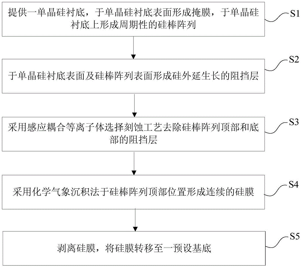
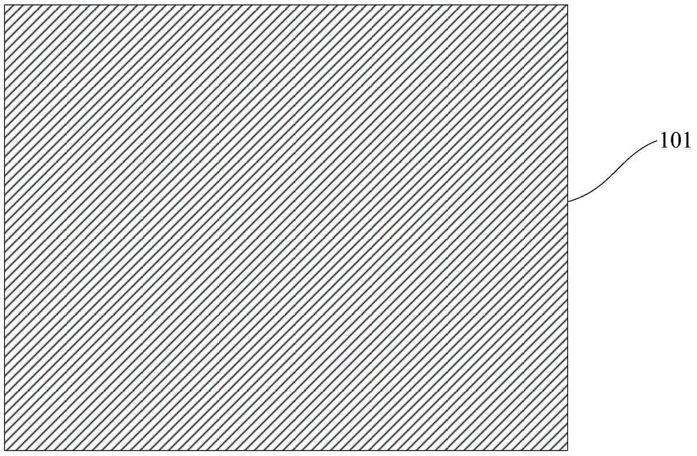
[0036] Embodiments of the present invention are described below through specific examples, and those skilled in the art can easily understand other advantages and effects of the present invention from the content disclosed in this specification. The present invention can also be implemented or applied through other different specific implementation modes, and various modifications or changes can be made to the details in this specification based on different viewpoints and applications without departing from the spirit of the present invention.

[0037] see Figure 1 to Figure 13 . It should be noted that the diagrams provided in this embodiment are only schematically illustrating the basic idea of ​​the present invention, and only the components related to the present invention are shown in the diagrams rather than the number, shape and shape of the components in actual implementation. Dimensional drawing, the type, quantity and proportion of each component can be changed ar...


PUM


Abstract

The invention provides a technology for preparing layer transfer thin crystal silicon by adopting a neighbor shadow effect auxiliary array method. The technology comprises the steps of: 1), forming a mask used for manufacturing a periodic rod array on the surface of a monocrystal silicon substrate, and forming a periodic silicon rod array on the monocrystal silicon substrate by adopting dry etching or epitaxial growth technology; 2) forming barrier layers on the surface of a monocrystal silicon substrate and the surface of the periodic silicon rod array; 3) exposing silicon at the top part of the periodic silicon rod array by adopting a selective etching technology; 4) taking the exposed silicon at the top end of the periodic silicon rod array as seed crystal or nucleation sites of epitaxial growth, and forming a continuous silicon film on the top part of the periodic silicon rod array by adopting a chemical vapor phase deposition method; 5) and stripping the silicon film, and transferring the silicon film to a preset substrate. The technology provided by the invention adopts a monocrystal silicon wafer as the mother substrate, the grown thin film can inherit the crystal quality of the mother board, and the high crystal quality of the thin film is ensured; the substrate can be reused after simple treatment when the thin film is stripped off, the chemical vapor phase deposition thin film growing technology is simple, and the production cost can be effectively reduced.

Description

technical field [0001] The invention belongs to the technical field of semiconductor materials, and in particular relates to a process for preparing layer-transferred thin-crystal silicon by a neighboring shadow effect auxiliary array method. Background technique [0002] The resource-rich, renewable and pollution-free solar energy is an extremely important option in the national new energy strategy. Due to mature silicon semiconductor process technology, abundant material resources, and high photoelectric conversion efficiency, crystalline silicon cells occupy more than 85% of the market share in the current photovoltaic industry. The fundamental reason for the high conversion efficiency of crystalline silicon cells lies in the high crystal quality, which ensures a high minority carrier lifetime and a long minority carrier diffusion length. However, the production of monocrystalline silicon wafers is a process of high energy consumption and high loss, which is the biggest ...

Claims


Application Information

Patent Timeline
IPC IPC(8): H01L21/02H01L21/78
CPCH01L21/02019H01L21/02381H01L21/02532H01L21/7813
Inventor 刘东方张伟刘洪超王聪陈小源杨辉
Owner SHANGHAI ADVANCED RES INST CHINESE ACADEMY OF SCI
Why Eureka
Try Eureka