

Metal oxide thin film transistor and manufacturing method thereof
An oxide thin film and oxide semiconductor technology, applied in transistors, semiconductor/solid-state device manufacturing, semiconductor devices, etc., can solve the problem of difficult to achieve industrialized production of thin film transistors with simple process, low cost and high stability, harsh experimental conditions, and high reliability. Problems such as poor repeatability, to achieve the effect of light stability, good uniformity, and improved stability
- Summary
- Abstract
- Description
- Claims
- Application Information
AI Technical Summary
Problems solved by technology
Method used
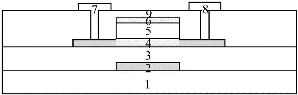
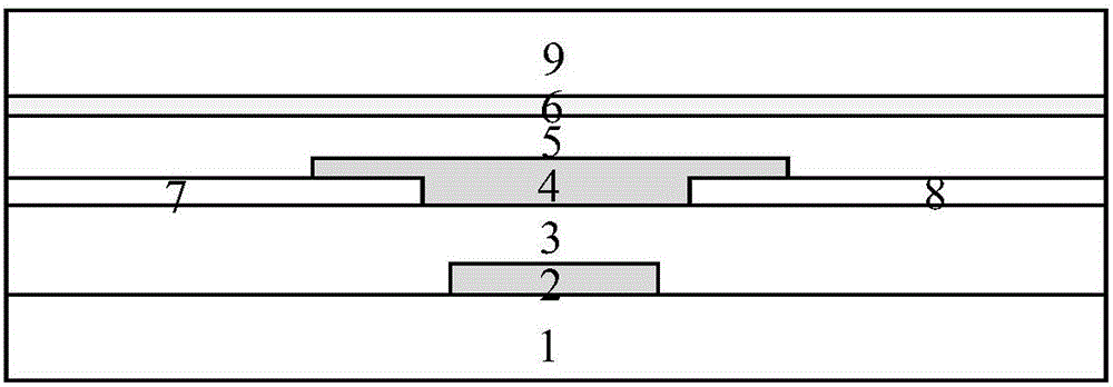
Image

Examples
example 1
[0032] A method for preparing a metal oxide thin film transistor, comprising the steps of:
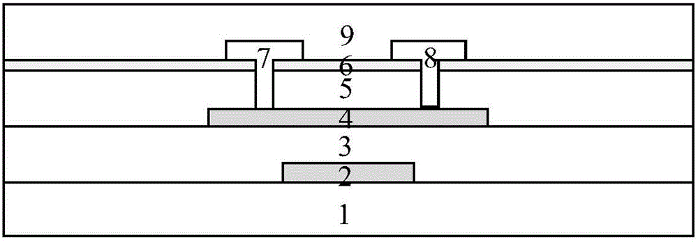
[0033] 1) Preparation of metal oxide semiconductor thin films: based on figure 1 Structure After the gate 2 and the gate insulating layer 3 are prepared, when the metal oxide semiconductor layer 4 is prepared by magnetron sputtering, the target material is indium gallium zinc oxide as an example, the deposition gas atmosphere is nitrogen and oxygen, and the ratio is 29.4 : 0.6sccm, the deposition temperature is 150°C, the deposition power is 180W, the deposition pressure is 1Pa, and the deposition thickness is 50nm.
[0034] 2) Refer to figure 1Then a barrier layer 5 is prepared with a thickness of 100 nm.
[0035] 3) Preparation of fluorine-doped silicon nitride thin film layer 6: After step 2), fluorine-doped silicon nitride is prepared by plasma-enhanced chemical vapor deposition, and the deposition gas atmosphere is silicon tetrafluoride, nitrous oxide, and nitrogen. The flow ra...
example 2
[0041] A method for preparing a metal oxide thin film transistor, comprising the steps of:
[0042] 1) Preparation of metal oxide semiconductor thin films: based on figure 1 Structure After the gate 2 and the gate insulating layer 3 are prepared, when the metal oxide semiconductor layer 4 is prepared by non-vacuum chemical vapor deposition, taking indium zinc oxide as an example, the precursor liquid is zinc fluoride and indium acetate, and the solvent is water and methanol , 10 and 90 mL respectively, stirred at room temperature for 3 hours, and then filtered through a 0.2 μm filter. The deposition conditions are as follows, the deposition gas is air, the deposition temperature is 350° C., and the deposition thickness is 45 nm.
[0043] 2) Refer to figure 1 Then a barrier layer 5 is prepared with a thickness of 50 nm.
[0044] 3) Preparation of nitrogen-doped silicon oxide thin film layer 6: After step 2), nitrogen-doped silicon oxide is prepared by magnetron sputtering, t...
example 3
[0050] A method for preparing a metal oxide thin film transistor, comprising the steps of:
[0051] 1) Preparation of metal oxide semiconductor thin films: based on figure 1 Structure After preparing the gate 2 and the gate insulating layer 3, when preparing the metal oxide semiconductor layer 4 by spin coating, taking indium zinc oxide as an example, the precursor solution is 0.1M zinc acetate, 0.1M indium nitrate, the solvent is water, and the room temperature Stir for 3 hours, then filter with a 0.2 μm filter. After that, it was spin-coated at 4000rpm for 30s, and then heat-treated at 250°C for 1 hour in air atmosphere.
[0052] 2) Refer to figure 1 Then a barrier layer 5 is prepared with a thickness of 150 nm.
[0053] 3) Preparation of hydrogen-doped silicon nitride thin film layer 6: After step 2), hydrogen-doped silicon nitride is prepared by plasma enhanced chemical vapor deposition. The deposition gas atmosphere is silicon tetrafluoride, ammonia, nitrogen, and the ...
PUM
| Property | Measurement | Unit |
|---|---|---|
| Thickness | aaaaa | aaaaa |
Abstract
Description
Claims
Application Information