

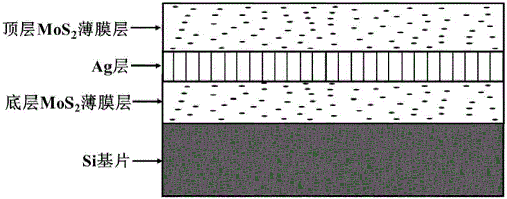
A MoS2/Ag/MoS2 semiconductor film material and a preparing method thereof
A thin film material and semiconductor technology, applied in metal material coating process, ion implantation plating, coating and other directions, can solve product performance consistency, poor stability, material structure and performance instability, and product quality control difficulties Large and other problems, to achieve the effect of strong performance repeatability, stable structure, and improved uniformity and continuity
- Summary
- Abstract
- Description
- Claims
- Application Information
AI Technical Summary
Problems solved by technology
Method used
Image

Examples
Embodiment 1
[0066] The preparation method is as follows:
[0067] The first step, silicon substrate surface cleaning step
[0068] Select an intrinsically insulating and non-conductive Si single crystal substrate, and ultrasonically clean it in alcohol, acetone and deionized water for 180s;
[0069] Remove and blow dry with dry nitrogen;
[0070] The second step, the underlying MoS 2 Thin film layer surface deposition step
[0071] Put the cleaned Si single crystal substrate into a tray, put it into a vacuum chamber, and evacuate the vacuum chamber to a high vacuum, and adjust the temperature of the Si single crystal substrate to the first temperature of 200°C in an argon atmosphere , the argon gas pressure was adjusted to the first pressure of 3Pa, using DC magnetron sputtering technology, under the condition of constant 30W sputtering power, the ionized ions were used to bombard MoS 2 A ceramic target, on the upper surface of the Si substrate, deposit a layer of MoS with a thickness...
Embodiment 2
[0082] Description: This example is a comparative example, and the target product is pure MoS 2 Thin film material, no intermediate Ag intercalation.
[0083] The preparation method is as follows:
[0084] The first step, silicon substrate surface cleaning step
[0085] Select an intrinsically insulating and non-conductive Si single crystal substrate, and ultrasonically clean it in alcohol, acetone and deionized water for 180s;
[0086] Remove and blow dry with dry nitrogen;
[0087] The second step, the underlying MoS 2 Thin film layer surface deposition step
[0088] Put the cleaned Si single crystal substrate into a tray, put it into a vacuum chamber, and evacuate the vacuum chamber to a high vacuum, and adjust the temperature of the Si single crystal substrate to the first temperature of 200°C in an argon atmosphere , the argon gas pressure was adjusted to the first pressure of 3Pa, using DC magnetron sputtering technology, under the condition of constant 30W sputteri...
Embodiment 3
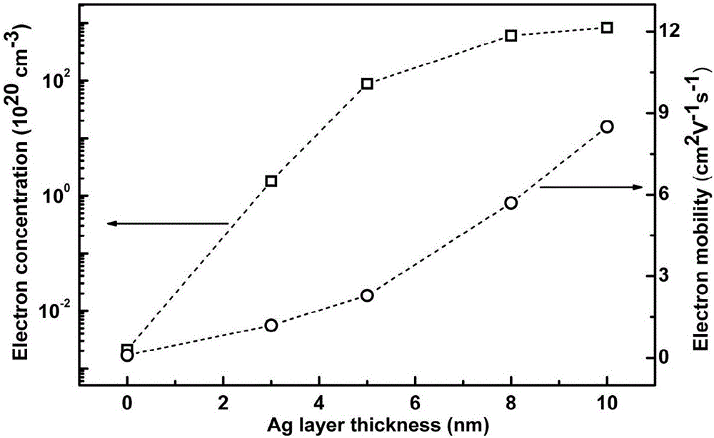
[0092] Only in the third step, the thickness of the Ag intercalation layer was adjusted to 3nm by adjusting the sputtering time;
[0093] Product performance test results:
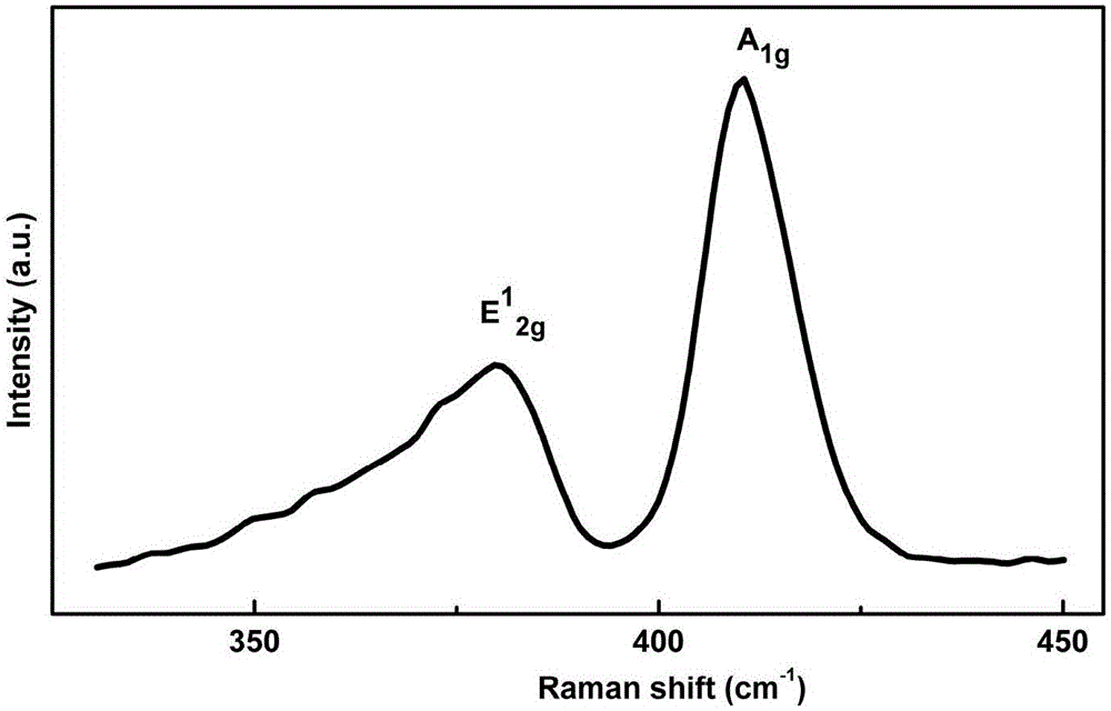
[0094] It has been tested that at room temperature (20-25°C), the prepared MoS 2 / Ag / MoS 2 The electron carrier concentration, electron mobility and resistivity values of the thin film material are 1.8×10 20 cm -3 、1.2cm 2 V -1 the s -1 and 9.8Ωcm.
PUM
| Property | Measurement | Unit |
|---|---|---|
| thickness | aaaaa | aaaaa |
| thickness | aaaaa | aaaaa |
| thickness | aaaaa | aaaaa |
Abstract
Description
Claims
Application Information