Back junction backcontact solar cell

A solar cell and back contact technology, applied in the field of solar cells, can solve problems such as increasing series resistance, increasing carrier recombination rate, and reducing battery performance

Inactive Publication Date: 2017-05-10
INST OF MICROELECTRONICS CHINESE ACAD OF SCI
View PDF3 Cites 14 Cited by
  • Summary
  • Abstract
  • Description
  • Claims
  • Application Information

AI Technical Summary

Problems solved by technology

However, a problem that most solar cells, including back-junction and back-contact solar cells, have not solved is that after the metal and the substrate form an ohmic contact, a large number of interface states will be introduced on the contact surface, which makes the carrier on the surface The recombination rate increases significantly, which can greatly reduce the performance of the battery
The usual solution is to minimize the contact area between the metal and the substrate, but this will cause the lateral transport of carriers, increase the series resistance, and reduce the performance of the battery.

Method used


Image

  • Back junction backcontact solar cell
  • Back junction backcontact solar cell
  • Back junction backcontact solar cell

Examples


Embodiment 1

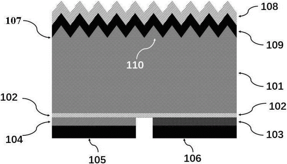
[0113] see figure 1 , figure 1 A schematic diagram of the structure of the back-junction and back-contact solar cell provided in Example 1 of the present invention. Among them, 101 is the substrate (substrate), 102 is the tunnel oxide layer, 103 is the N-type doped semiconductor layer, 104 is the P-type doped semiconductor layer, 105 is the positive electrode, 106 is the negative electrode, and 107 is the front electrode. In the field area, 108 is an anti-reflection layer, 109 is a passivation layer on the front surface, and 110 is an overall suede light-trapping structure.

[0114] Depend on figure 1 It can be seen that the P-type doped semiconductor layer and the N-type doped semiconductor layer are alternately distributed in the shape of interpolated fingers, and the P-type doped semiconductor layer and the N-type doped semiconductor layer are separated by a trench, and are insulated from each other. of. Wherein the P-type doped semiconductor layer as the emitter is wid...

Embodiment 2

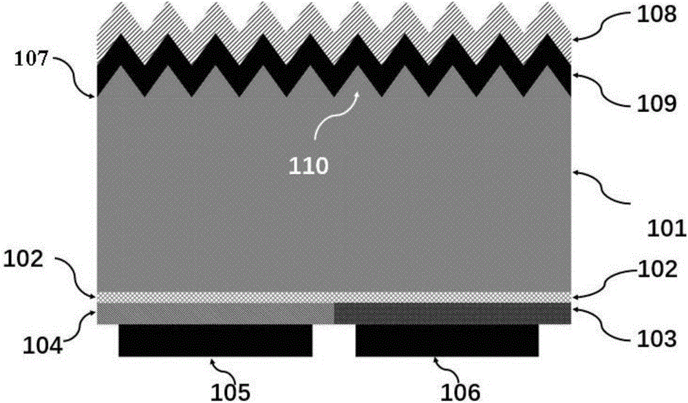
[0120] see figure 2 , figure 2 A schematic diagram of the structure of the back-junction and back-contact solar cell provided by Example 2 of the present invention. Among them, 101 is the substrate (substrate), 102 is the tunnel oxide layer, 103 is the N-type doped semiconductor layer, 104 is the P-type doped semiconductor layer, 105 is the positive electrode, 106 is the negative electrode, and 107 is the front electrode. In the field area, 108 is an anti-reflection layer, 109 is a passivation layer on the front surface, and 110 is an overall suede light-trapping structure.

[0121] Depend on figure 2 It can be seen that the P-type doped semiconductor layer and the N-type doped semiconductor layer can also be as figure 2 It is shown that they are connected together. Although they are connected together, the P-type doped semiconductor layer and the N-type doped semiconductor layer will form a PN junction. When the battery is working normally, the PN junction is in a reve...

Embodiment 3

[0128] The preparation method of the solar cell is as follows:

[0129] A pyramid-shaped suede structure is prepared by corroding the front surface of an N-type single crystal silicon wafer with a thickness of 100 microns with a sodium hydroxide solution. The concentration of sodium hydroxide is 1%, the etching time is 5 minutes, and the temperature is 60 ℃. On the textured surface, arsenic atoms were implanted by ion implantation to form an N-type doped region on the front surface with a doping concentration of 10 17 cm -3 , the doping depth is 2 microns. After forming the N-type doped region on the front surface, a layer of silicon oxide with a thickness of 20 nanometers is deposited on the front surface as a passivation layer by plasma-enhanced chemical vapor deposition, and then placed on the passivation layer by sputtering A layer of 200nm ITO was deposited as an anti-reflection layer by the way. Then use thermal oxygen oxidation method to form a tunnel oxide layer wi...


PUM


Abstract

The invention provides a back junction backcontact solar cell. The back junction backcontact solar cell comprises a substrate, a composite layer, a tunneling oxide layer, a P-type doped semiconductor layer, an N-type doped semiconductor layer, a positive electrode and a negative electrode, wherein the composite layer is combined on a front surface of the substrate, the tunneling oxide layer is combined on a back surface of the substrate, the P-type doped semiconductor layer and the N-type doped semiconductor layer are combined on the tunneling oxide layer, the positive electrode is arranged on the P-type doped semiconductor layer, and a negative electrode is arranged on the N-type doped semiconductor layer. The invention proposes a back junction backcontact solar cell employing a tunneling oxide layer passivation contact structure; with the adoption of the tunneling oxide layer passivation contact structure, direct contact of a metal electrode and the substrate is prevented, the combination of a carrier on a metal contact interface is effectively reduced, and an opening voltage of the cell is increased; and moreover, combination addition cannot brought by metal contact, the vast majority of areas of an emission field and a back field can be covered by metal contact, transverse transmission of the carrier is prevented, the series resistance is favorably reduced, and the cell efficiency is further improved.

Description

technical field [0001] The invention belongs to the technical field of solar cells, and relates to a back-junction and back-contact solar cell, in particular to a back-junction and back-contact solar cell with a tunnel oxide layer passivation contact structure on the back. Background technique [0002] A solar cell, also known as a "solar chip" or a "photovoltaic cell", is a photoelectric semiconductor sheet that uses sunlight to directly generate electricity. It is a device that directly converts light energy into electrical energy through the photoelectric effect or photochemical effect. As long as the solar cell is illuminated by light that meets a certain illuminance condition, it can output voltage instantly and generate current when there is a loop. In physics, it is called solar photovoltaic (Photovoltaic, abbreviated as PV), or photovoltaic for short. The working principle of a solar cell is that when sunlight shines on the p-n junction of a semiconductor, new hole-...

Claims


Application Information

Patent Timeline
Patent Type & Authority Applications(China)
IPC IPC(8): H01L31/0236H01L31/0352H01L31/0216H01L31/0224
CPCY02E10/50H01L31/02363H01L31/02167H01L31/022441H01L31/0352
Inventor 贾锐姜帅陶科孙恒超戴小宛金智刘新宇
Owner INST OF MICROELECTRONICS CHINESE ACAD OF SCI
Why Eureka
Try Eureka