High-molecular-weight polysilane and method for producing same

一种制造方法、聚硅烷的技术,应用在化学仪器和方法、半导体/固态器件制造、硅等方向,能够解决聚硅烷结晶性低、平均分子量小、无法得到高导电性等问题

Active Publication Date: 2017-05-10
THIN FILM ELECTRONICS ASA
View PDF9 Cites 1 Cited by
  • Summary
  • Abstract
  • Description
  • Claims
  • Application Information

AI Technical Summary

Problems solved by technology

[0009] However, there is a problem that since the above-mentioned polysilane or silicon-containing polymer has a small average molecular weight, the dehydrogenated polysilane obtained by firing has low crystallinity, and high conductivity cannot be obtained.

Method used


Image

  • High-molecular-weight polysilane and method for producing same
  • High-molecular-weight polysilane and method for producing same
  • High-molecular-weight polysilane and method for producing same

Examples


Embodiment 1

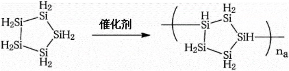
[0097] Example 1 (Synthesis of Polycyclopentasilane by Polymerization of Cyclopentasilane Using a Palladium Catalyst Loaded on a Polymer)

[0098] In an inert atmosphere, cyclopentasilane (0.8 g) was added to 0.44 mol % of a commercially available polymer-supported palladium catalyst (manufactured by Wako Pure Chemical Industries, Ltd., trade name PIPd (Pd content 3 mass %), 82.1 mg) glass sample tube, the reaction mixture was stirred for 1 hour in an uncorked sample tube. Next, the reaction was terminated with 5.14 g of cyclohexane to precipitate insoluble components, and the mixture was filtered through a polytetrafluoroethylene membrane filter with a pore diameter of 0.45 μm. Next, the solution was transferred to a pear-shaped flask, and volatile components were removed by reducing pressure (about 20 Torr or less, for example, 1 to 20 Torr). The product can be stored as an 8% by mass solution dissolved in distilled cyclooctane. As a result of measuring the product by gel ...


PUM

PropertyMeasurementUnit
aperture sizeaaaaaaaaaa
weight-average molecular weightaaaaaaaaaa

Abstract

[Problem] To produce an application-type polysilane composition using polysilane having a high weight-average molecular weight, and provide an excellent silicon thin film having high conductivity after applying the polysilane composition to a substrate and firing the substrate. [Solution] Polysilane having a weight-average molecular weight of from 5,000 to 8,000. The polysilane is a polymer of cyclopentasilane. A silicon film obtained by applying a polysilane composition of polysilane dissolved in a solvent to a substrate, and firing at from 100 degrees to 425 degrees. Polymerization of cyclopentasilane is carried out in the presence of a polymer-supported palladium catalyst. In the polymer-supported palladium catalyst, the palladium of the catalyst component is immobilized by functionalized polystyrene. The palladium comprises a palladium compound or a palladium complex. Immobilization of the palladium involves the microencapsulation of a zero-valent palladium complex or divalent palladium compound using functionalized polystyrene. The zero-valent palladium complex comprises a tetrakis(triphenylphosphine)palladium(0) complex.

Description

technical field [0001] The present invention relates to high molecular weight polysilane and its production method. Furthermore, the present invention also relates to silane polymers used in applications such as integrated circuits and thin film transistors. Background technique [0002] A silicon semiconductor is a material that has been researched as a material for a thin film transistor (TFT) or a solar cell. [0003] In patterning a silicon thin film applied to an integrated circuit or a thin film transistor, the silicon film is usually formed by a vacuum process such as a CVD method. Since such a device uses a vacuum process, a large-scale device is required, and there are problems such as difficulty in handling because the raw material is gas. [0004] In order to solve these problems, there is a method of forming a silicon film by dehydrogenating a silane polymer dissolved in an organic solvent after applying it to a substrate and firing it. [0005] For example, a...

Claims


Application Information

Patent Timeline
Patent Type & Authority Applications(China)
IPC IPC(8): C01B33/04C01B33/02C03C17/22C08G77/60
CPCC01B33/021C08G77/60C09D183/16C01B33/02C01B33/04C03C17/22C03C17/32C08G77/08C08K9/10B05D3/0254C09D5/24H01L21/02532
Inventor 远藤雅久孙军后藤裕一永井健太郎
Owner THIN FILM ELECTRONICS ASA
Why Eureka
Try Eureka