Silicon carbide vertical insulated gate bipolar transistor and production method thereof

A bipolar transistor and insulated gate technology, applied in the field of microelectronics, can solve the problems of increasing conduction power loss, weakening the conductance modulation effect, and being unfavorable for the parallel application of devices, so as to improve the switching speed of devices and reduce the switching loss of devices Effect

Inactive Publication Date: 2017-05-24
XIDIAN UNIV
View PDF5 Cites 2 Cited by
  • Summary
  • Abstract
  • Description
  • Claims
  • Application Information

AI Technical Summary

Problems solved by technology

However, this method also weakens the conductance modulation effect of the device when it is turned on, and increases the conduction power loss.
More importantly, the local carrier lifetime modulation technique will make the device on-resistance have a negative temperature coefficient, which is not conducive to the parallel application of devices under high current

Method used


Image

  • Silicon carbide vertical insulated gate bipolar transistor and production method thereof
  • Silicon carbide vertical insulated gate bipolar transistor and production method thereof
  • Silicon carbide vertical insulated gate bipolar transistor and production method thereof

Examples


Embodiment 1

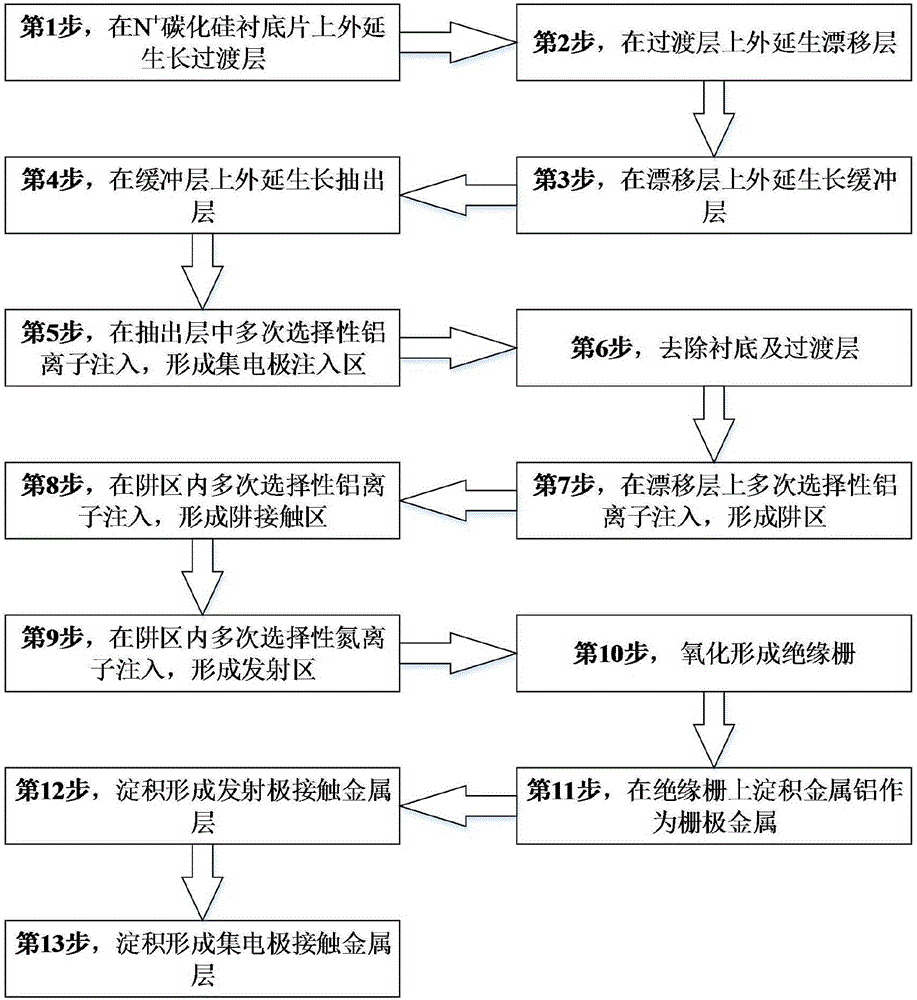
[0033] Step 1, epitaxially grow the transition layer on the N+ silicon carbide substrate, such as image 3 As shown, the N+ type silicon carbide substrate is first cleaned by RCA standard; then a transition layer with a thickness of 20 μm is epitaxially grown on the front side of the N+ type silicon carbide substrate by low pressure hot wall chemical vapor deposition.

[0034] It should be noted that the growth conditions of the transition layer are: the temperature is 1600° C., the pressure is 100 mbar, the reaction gas is silane and propane, and the carrier gas is pure hydrogen.

[0035] It should be noted that the RCA standard cleaning method was first created by Kern and Puotinen in the RCA laboratory of N.J.Princeton in 1965, and thus got its name. RCA is a typical wet chemical cleaning method that is still the most commonly used. The cleaning method mainly includes the following cleaning solutions.

[0036] (1), SPM:H 2 SO 4 / H 2 o 2 120~150℃ SPM has high oxidation ...


PUM

PropertyMeasurementUnit
thicknessaaaaaaaaaa
thicknessaaaaaaaaaa
thicknessaaaaaaaaaa

Abstract

The invention discloses a silicon carbide vertical insulated gate bipolar transistor and a production method thereof, and belongs to the microelectronic technology field. Pumping of excess minority carrier in a drifting layer during switching-off of a device is effectively facilitated, and the switching-on/off speed of the device is improved, and the loss of the switch is reduced, and therefore the integrated energy loss of the device in high frequency application is obviously reduced. An on-resistance negative temperature coefficient phenomenon caused by a local carrier service lifetime modulation technology used in the buffer layer of the device is prevented, and the reliability of the parallel connection application of the devices under a large current condition is improved. A pumping layer is disposed in an injection region of a collector, and the periphery of the pumping layer is connected with the injection region of the collector, and in addition, the top end of the pumping layer is connected with the bottom layer of the buffer layer, and then the bottom part of the pumping layer is connected with the top part of the collector contacted with metal.

Description

technical field [0001] The invention belongs to the technical field of microelectronics and relates to semiconductor devices, in particular to a silicon carbide vertical insulated gate bipolar transistor and a preparation method thereof. Background technique [0002] The rapid development of modern power electronics and new energy technologies has put forward higher and higher requirements for high-power semiconductor devices. Due to material limitations, traditional silicon devices are difficult to operate at high temperatures above 250°C, especially when high operating temperatures coexist with high power, high frequency, and strong radiation environments. [0003] Silicon carbide is a wide bandgap semiconductor material developed rapidly in the past ten years. Its main features are: large bandgap width, high breakdown electric field, high thermal conductivity, and high electron saturation drift speed. This determines that it has good properties of working under high temp...

Claims


Application Information

Patent Timeline
Patent Type & Authority Applications(China)
IPC IPC(8): H01L29/739H01L21/331H01L29/06
CPCH01L29/06H01L29/66257H01L29/66325H01L29/7393
Inventor 宋庆文唐冠南元磊汤晓燕张艺蒙张玉明
Owner XIDIAN UNIV
Why Eureka
Try Eureka