Electroless tin plating formula for printed circuit board

A printed circuit board, chemical tin plating technology, applied in liquid chemical plating, metal material coating process, coating and other directions, can solve the problems of easy penetration plating, chemical nickel gold nickel corrosion, high storage conditions, etc. The coating is flat and dense, reducing adverse effects and excellent compatibility

Active Publication Date: 2017-07-11
SHENZHEN CHENGGONG CHEM
View PDF3 Cites 10 Cited by
  • Summary
  • Abstract
  • Description
  • Claims
  • Application Information

AI Technical Summary

Problems solved by technology

[0003] The surface treatment in the circuit board field mainly refers to the final treatment of the copper surface. The treated surface can perform functions such as welding and binding. In this field, developed countries have been at the forefront. In recent years, OSP, chemical nickel and gold It has developed to a certain extent in China, but OSP finished product inspection is not convenient for visual inspection and electrical measurement, SMT rework is not suitable, and storage conditions are required.
Electroless nickel gold has the disadvantages of nickel corrosion, easy permeation plating, missing plating, etc.
[0004] Chemically pure tin coating has long been used in the field of surface treatment of automotive circuit boards or IC substrates, thanks to its many advantages, such as good flatness of the tin surface, excellent electrical conductivity and solderability, and can be used many times Soldering, the tin layer does not contain lead, no pollution to the environment, long storage period (one year), simple manufacturing process, good working environment, etc., but the existing coating morphology has loose coating, no obvious crystallization, and relatively high porosity High disadvantage

Method used


Image

  • Electroless tin plating formula for printed circuit board
  • Electroless tin plating formula for printed circuit board
  • Electroless tin plating formula for printed circuit board

Examples


Embodiment 1

[0054] Stannous ion: 10g / L;

[0055] Thiourea: 70g / L;

[0056] Methanesulfonic acid: 70g / L;

[0057] Citric acid: 30g / L;

[0058] Tetrasodium iminodisuccinate: 50g / L;

[0059] Carbohydrazide: 30g / L;

[0060] Sodium dodecylbenzenesulfonate: 10mg / L;

[0061] Bismuth acetate: 0.15g / L;

[0062] Polyamino polyether methylene phosphonic acid: 20g / L;

[0063] The bath temperature is 65°C; the time is 15 minutes;

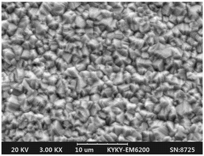
[0064] The thickness of the obtained coating is 0.84 μm, and the surface morphology of the coating is as follows figure 1 shown, from figure 1 It can be seen from the figure that the industry generally requires the thickness of the electroless tin coating to be above 0.8 microns. The thickness of the coating under this formula and parameter conditions meets the requirements of the industry, and the crystallization of the coating is clear and dense.

Embodiment 2

[0066] Stannous ion: 30g / L;

[0067] Thiourea: 130g / L;

[0068] Methanesulfonic acid: 30g / L;

[0069] Citric acid: 60g / L;

[0070] Tetrasodium iminodisuccinate: 20g / L;

[0071] Carbohydrazide: 10g / L;

[0072] Sodium dodecylbenzenesulfonate: 50mg / L;

[0073] Bismuth acetate: 0.05g / L;

[0074] Polyamino polyether methylene phosphonic acid: 40g / L;

[0075] The bath temperature is 70°C; the time is 15 minutes;

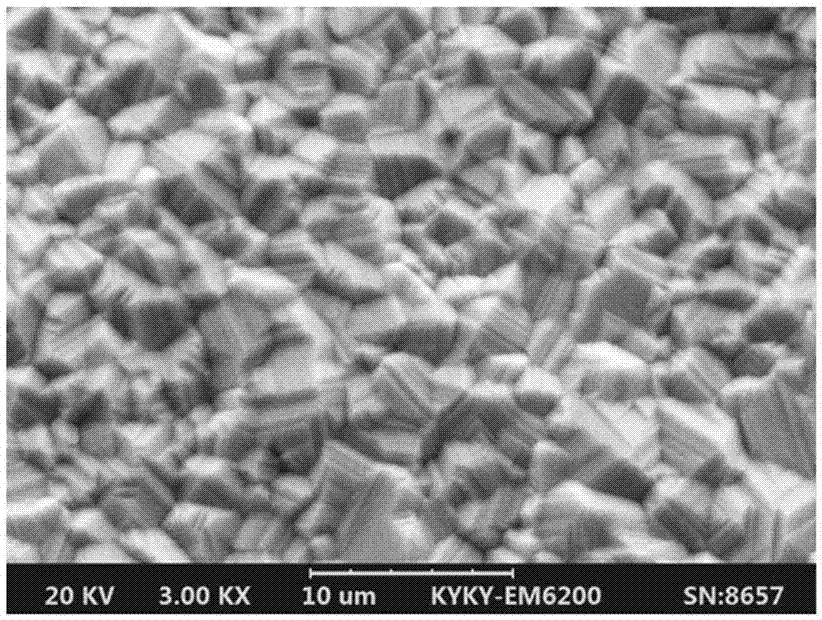
[0076] The thickness of the obtained coating is 1.34 μm, and the surface morphology of the coating is as follows figure 2 shown, from figure 2 It can be seen from the figure that the industry generally requires the thickness of the electroless tin coating to be above 0.8 microns, and the thickness of the coating under this formula and parameter conditions meets the requirements of the industry, and the crystallization of the coating is clear and dense.

Embodiment 3

[0078] Stannous ion: 20g / L;

[0079] Thiourea: 100g / L;

[0080] Methanesulfonic acid: 45g / L;

[0081] Citric acid: 50g / L;

[0082] Tetrasodium iminodisuccinate: 35g / L;

[0083] Carbohydrazide: 15g / L;

[0084] Sodium lauryl sulfate: 45mg / L;

[0085] Bismuth acetate: 0.1g / L;

[0086] Polyamino polyether methylene phosphonic acid: 30g / L;

[0087] The bath temperature is 75°C; the time is 15 minutes;

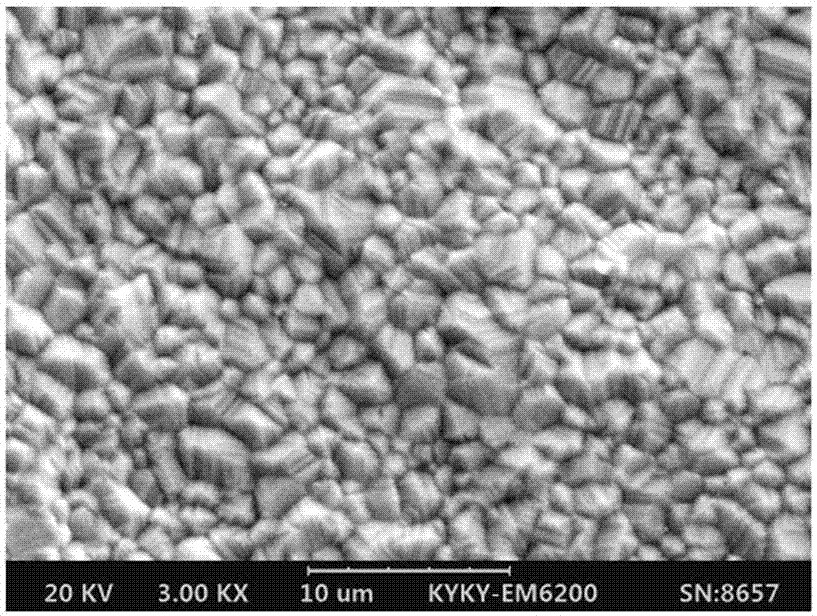
[0088] The thickness of the coating is 1.28 μm, and the surface morphology of the coating is as follows image 3 shown, from image 3 It can be seen from the figure that the industry generally requires the thickness of the electroless tin coating to be above 0.8 microns. The thickness of the coating under this formula and parameter conditions meets the requirements of the industry, and the crystallization of the coating is clear and dense.

[0089] As a comparative example: use a commercially available chemical tin plating solution to carry out chemical tin plating, the tem...


PUM

PropertyMeasurementUnit
thicknessaaaaaaaaaa
thicknessaaaaaaaaaa
thicknessaaaaaaaaaa

Abstract

The invention discloses an electroless tin plating formula for a printed circuit board. The formula comprises the following components with the following concentrations: 10-30g / L of stannous ions, 70-130g / L of thiourea, 30-70g / L of methanesulfonic acid, 30-60g / L of citric acid, 20-50g / L of tetrasodium iminodisuccinate, 10-30g / L of carbohydrazide, 10-50mg / L of interfacial agent, 0.05-0.15g / L of bismuth acetate and 20-40g / L of polyamino polyether methylene phosphonate, wherein the component solutions are uniformly mixed and then prepared into an electroless tin plating solution; and the electroless tin plating solution has the following characteristics: tin is stable in tin deposition rate, bivalent tin is not liable to be oxidized into tetravalent tin, and the solution is high in stability. The formula disclosed by the invention contains many complexing agents, the stannous ions are not liable to be oxidized into tetravalent tin, the oxidization of oxygen dissolved in the plating solution can be cancelled by virtue of a reducing agent, the plating solution contains bismuth acetate, a plating layer is a tin-bismuth alloy, and the alloyed plating layer is not liable to grow tin whiskers; and moreover, the electroless tin plating solution has the following characteristics: tin is stable in tin deposition rate, bivalent tin is not liable to be oxidized into tetravalent tin, and the solution is high in stability.

Description

technical field [0001] The invention relates to the technical field of circuit boards, in particular to an electroless tin plating formula for printed circuit boards. Background technique [0002] Printed circuit board, also known as PCB circuit board, is the provider of electrical connection for electronic components. Printed circuit boards have developed from single-layer to double-sided, multi-layer and flexible boards, and are constantly developing in the direction of high precision, high density and high reliability. Continuous reduction in size, cost reduction, and performance improvement enable printed circuit boards to maintain strong vitality in the development of future electronic products. The future development trend of printed circuit board manufacturing technology is to develop in the direction of high density, high precision, fine aperture, thin wire, small pitch, high reliability, multi-layer, high-speed transmission, light weight, and thin profile in terms ...

Claims


Application Information

Patent Timeline
Patent Type & Authority Applications(China)
IPC IPC(8): C23C18/52C23C18/48
CPCC23C18/1639C23C18/166C23C18/1683C23C18/48C23C18/52
Inventor 王江锋沈文宝
Owner SHENZHEN CHENGGONG CHEM
Why Eureka
Try Eureka