A method for realizing exciton laser emission of gallium telluride (gate) two-dimensional material

A two-dimensional material, laser emission technology, applied in phonon exciters, chemical instruments and methods, lasers, etc., can solve the problems of weakened spontaneous emission capability, unsuitable technology for industrialization, and reduced spontaneous emission capability.

Inactive Publication Date: 2019-05-10
SUN YAT SEN UNIV
View PDF1 Cites 0 Cited by
  • Summary
  • Abstract
  • Description
  • Claims
  • Application Information

AI Technical Summary

Problems solved by technology

[0005] One: the pollution introduced during the transfer of the single-layer chalcogenide material to the target device and the damage of the chalcogenide material itself. Obviously, the pollution is easy to cause the weakening of the spontaneous emission ability and the introduction of uncontrollable and unexplainable other Therefore, the damage of the material (such as wrinkles) weakens the ability of electron holes to propagate inside the material, thereby reducing the ability of spontaneous emission
[0006] Second: the target devices used, such as photonic crystals and HSQ / Si 3 N 4 The manufacture of microcavities is a rather complicated process, and the success rate and cost will increase exponentially, which is not suitable for the industrialization of technology

Method used


Image

  • A method for realizing exciton laser emission of gallium telluride (gate) two-dimensional material
  • A method for realizing exciton laser emission of gallium telluride (gate) two-dimensional material
  • A method for realizing exciton laser emission of gallium telluride (gate) two-dimensional material

Examples


Embodiment 1

[0035] A method for realizing GaTe two-dimensional material exciton laser emission, comprising steps:

[0036] The first step is to clean the sapphire wafer and quartz boat. First, put a sapphire substrate with a size of 1×1cm, a thickness of 0.5mm, and a surface roughness of 0.2nm into a beaker filled with 50ml of ethanol, perform ultrasonic cleaning for 15 minutes, and take it out and blow it dry with a nitrogen gun; Next, put the dried sapphire substrate into another beaker containing 50 ml of acetone, perform ultrasonic cleaning for 15 minutes, take it out and dry it with a nitrogen gun; finally put the dried sapphire substrate into 100 ml of deionized In water, perform ultrasonic cleaning for 10 minutes, take it out and dry it with a nitrogen gun.

[0037]In the second step, the sapphire substrate is annealed. The sapphire substrate cleaned up in the first step is directly put into the double-temperature zone CVD furnace tube produced by Tianjin Zhonghuan Company used ...

Embodiment 2

[0048] A method for realizing GaTe two-dimensional material exciton laser emission, comprising steps:

[0049] The first step is to clean the sapphire wafer and quartz boat. First, put a sapphire substrate with a size of 1×1cm, a thickness of 0.5mm, and a surface roughness of 0.2nm into a beaker filled with 50ml of ethanol, perform ultrasonic cleaning for 15 minutes, and take it out and blow it dry with a nitrogen gun; Next, put the dried sapphire substrate into another beaker containing 50 ml of acetone, perform ultrasonic cleaning for 15 minutes, take it out and dry it with a nitrogen gun; finally put the dried sapphire substrate into 100 ml of deionized In water, perform ultrasonic cleaning for 10 minutes, take it out and dry it with a nitrogen gun.

[0050] In the second step, the sapphire substrate is annealed. The sapphire substrate cleaned up in the first step is directly put into the double-temperature zone CVD furnace tube produced by Tianjin Zhonghuan Company used...

Embodiment 3

[0057] A method for realizing GaTe two-dimensional material exciton laser emission, comprising steps:

[0058] The first step is to clean the sapphire wafer and quartz boat. First, put a sapphire substrate with a size of 1×1cm, a thickness of 0.5mm, and a surface roughness of 0.2nm into a beaker filled with 50ml of ethanol, perform ultrasonic cleaning for 15 minutes, and take it out and blow it dry with a nitrogen gun; Next, put the dried sapphire substrate into another beaker containing 50 ml of acetone, perform ultrasonic cleaning for 15 minutes, take it out and dry it with a nitrogen gun; finally put the dried sapphire substrate into 100 ml of deionized In water, perform ultrasonic cleaning for 10 minutes, take it out and dry it with a nitrogen gun.

[0059] In the second step, the sapphire substrate is annealed. The sapphire substrate cleaned up in the first step is directly put into the double-temperature zone CVD furnace tube produced by Tianjin Zhonghuan Company used...


PUM

PropertyMeasurementUnit
purityaaaaaaaaaa
particle size (mesh)aaaaaaaaaa

Abstract

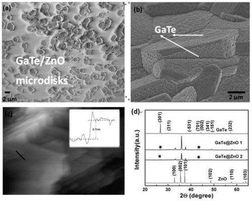
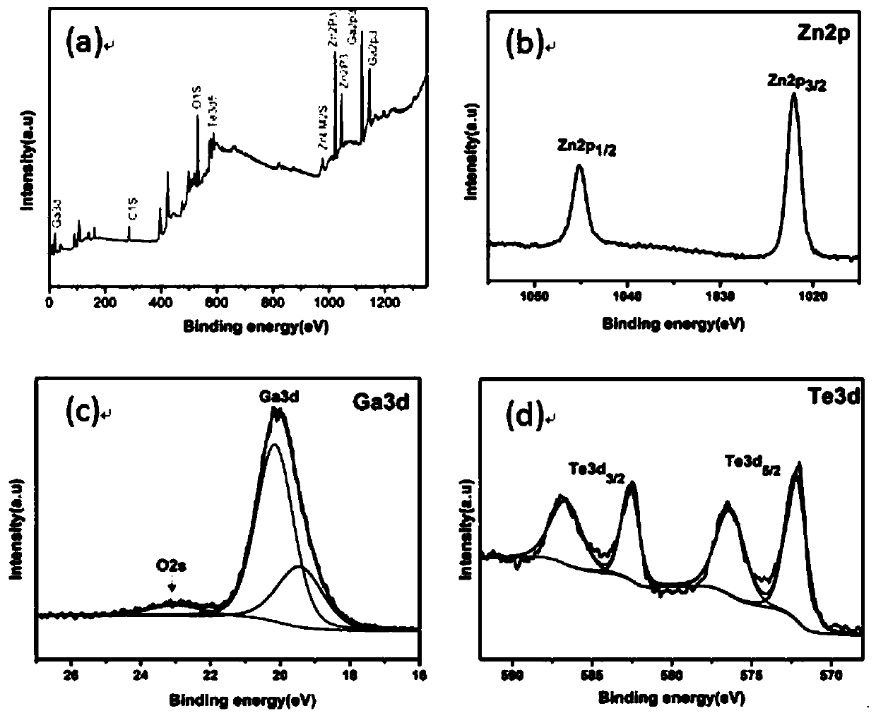
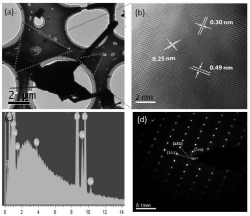
The invention discloses a method for achieving gallium telluride (GaTe) two-dimensional material exciton laser emission. The method comprises the following process steps: a) preparing a zinc oxide (ZnO) hexagonal micrometer disk on a sapphire substrate, and taking the zinc oxide (ZnO) hexagonal micrometer disk as a resonant cavity of GaTe material lasing; b) synthesizing a GaTe material on the sapphire substrate where the ZnO hexagonal micrometer disk grows, and taking the GaTe material as a gain material of the lasing; and c) representing a synthesized composite structure by using a scanning electronic microscope, Raman, an atomic force microscope, a transmission electron microscope and other representation means, and then testing a luminous property of GaTe under 532nm femtosecond laser pumping. A dimension of the ZnO hexagonal micrometer disk, a thickness of the GaTe material and other parameters are controlled through adjustments for gas flow, temperature and other conditions. The method has the advantages of high efficiency and the controllable synthesis, and the GaTe / ZnO hexagonal micrometer disk obtained through preparation has the high crystallization quality; and a further study on the synthesis of the new two-dimensional material GaTe is possessed, and GaTe single-layer exciton laser emission is also achieved at the first time.

Description

technical field [0001] The invention relates to the field of nanomaterial preparation and nanolaser, in particular to a method for realizing gallium telluride (GaTe) two-dimensional material exciton laser emission. Background technique [0002] As a new type of p-type sulfide, GaTe has a high hole density (6×10 12 cm -2 ), unlike other transition metal sulfides, its bulk material and atomic layer material both have a direct band gap (1.65eV) at room temperature. Gallium telluride belongs to the monoclinic crystal system (C 2 / m space group), the hexagonal phase is its metastable phase. Like other two-dimensional materials, the atoms in the GaTe layer are bonded by covalent bonds, while the interlayers are bonded by weak van der Waals force. Its layer is composed of Te-Ga-Ga-Te along the c-axis. The suitable energy band width makes it have potential applications in solar window materials and room temperature radiation detection, but because of its complex crystal structur...

Claims


Application Information

Patent Timeline
Patent Type & Authority Patents(China)
IPC IPC(8): H01S3/16C04B41/00C01G9/02C01B19/00
CPCC01B19/007C01G9/02C01P2002/72C01P2002/82C01P2004/03C01P2004/04C01P2006/60C04B41/0072H01S3/1606H01S3/169
Inventor 陈祖信楚盛
Owner SUN YAT SEN UNIV
Why Eureka
Try Eureka