Method for preparing barium-titanate ferroelectric nano-film based on pulsed electron beam deposition technology
A technology of pulsed electron beam and barium titanate is applied in the field of microelectronics to achieve the effect of reducing impurities, saving preparation costs and cleaning the surface
- Summary
- Abstract
- Description
- Claims
- Application Information
AI Technical Summary
Problems solved by technology
Method used
Image
Examples
Embodiment 1
[0050] Take a four-inch silicon wafer and cut it into a size of 1cm*1cm, put it in acetone, isopropanol, and ethanol for 15 minutes respectively (ultrasonic power 300W), and then dry it with nitrogen. The cleaned silicon wafer is placed in the pulse e-book deposition chamber, fixed with the substrate with silver glue, and the growth of barium titanate nano-ferroelectric thin film is carried out. The specific steps are as follows:
[0051]1) Clean up the reaction chamber pollutants:
[0052] Put the barium titanate target and the target substrate into the reaction chamber of the pulsed electron beam deposition system, and evacuate the chamber at a molecular pump speed of 1000 Hz until the vacuum degree reaches 1.0×10 -6 Torr or below;
[0053] 2) Control the partial pressure of oxygen in the reaction chamber:
[0054] Slow down the molecular pump to keep it at 250 Hz, then fill the chamber with oxygen to keep the chamber pressure at 6×10 -3 Torr;
[0055] 3) Growth of bariu...
Embodiment 2
[0067] A four-inch silicon wafer was cut into a size of 1 cm*1 cm, and placed in acetone, isopropanol, and ethanol for ultrasonic cleaning (ultrasonic power 300W) for 15 minutes each, and then dried with nitrogen. The cleaned silicon wafer is placed in the pulse e-book deposition chamber, fixed with the substrate with silver glue, and the barium titanate nano-ferroelectric film is grown, except for step 3) to grow the barium titanate film, the target temperature is 500 ℃, The heating rate is 5-20°C / min, and the rest of the steps are the same as in Example 1.
[0068] The barium titanate nano ferroelectric thin film obtained in this embodiment is characterized and tested:
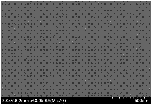
[0069] Image 6 The image of the surface of the barium titanate nanoferroelectric thin film obtained for this example under a scanning electron microscope shows that the surface of the thin film is relatively smooth.
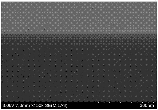
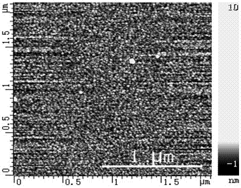
[0070] Figure 7 The image of the surface of the barium titanate nanoferroelectric thin...
Embodiment 3
[0073] Cut a four-inch silicon wafer into a size of 1 cm*1 cm, and place it in acetone, isopropanol, and ethanol for ultrasonic cleaning (ultrasonic power 300W) for 15 minutes each, and then dry it with nitrogen. The silicon wafer after cleaning is placed in the deposition chamber of the pulse e-book, and it is fixed with the substrate with silver glue, and the growth of barium titanate nano-ferroelectric thin film is carried out, except in step 3) in the growth of barium titanate thin film, the electron gun voltage is set as 10 KV, the number of pulses is 13000, the frequency is 5Hz, and the rest of the steps are the same as in Example 1.
[0074] The barium titanate nano ferroelectric thin film obtained in this embodiment is characterized and tested:
[0075] Figure 9 The image of the surface of the barium titanate nano ferroelectric film obtained for this example under a scanning electron microscope shows that there are obvious crystal grains on the surface of the film, w...
PUM
| Property | Measurement | Unit |
|---|---|---|
| Thickness | aaaaa | aaaaa |
Abstract
Description
Claims
Application Information
 - R&D
- Intellectual Property
- Life Sciences
- Materials
- Tech Scout
- Unparalleled Data Quality
- Higher Quality Content
- 60% Fewer Hallucinations
Browse by: Latest US Patents, China's latest patents, Technical Efficacy Thesaurus, Application Domain, Technology Topic, Popular Technical Reports.
© 2025 PatSnap. All rights reserved.Legal|Privacy policy|Modern Slavery Act Transparency Statement|Sitemap|About US| Contact US: help@patsnap.com


