Organic semiconductor laser material and preparation method and application thereof
A technology of organic semiconductor and laser materials, which is applied in the field of organic semiconductor laser materials and its preparation, and can solve the problems of large multi-photon absorption cross section
- Summary
- Abstract
- Description
- Claims
- Application Information
AI Technical Summary
Problems solved by technology
Method used
Image

Examples
Embodiment 1
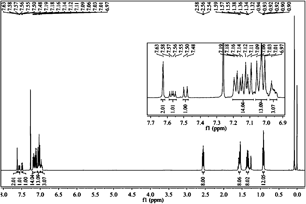
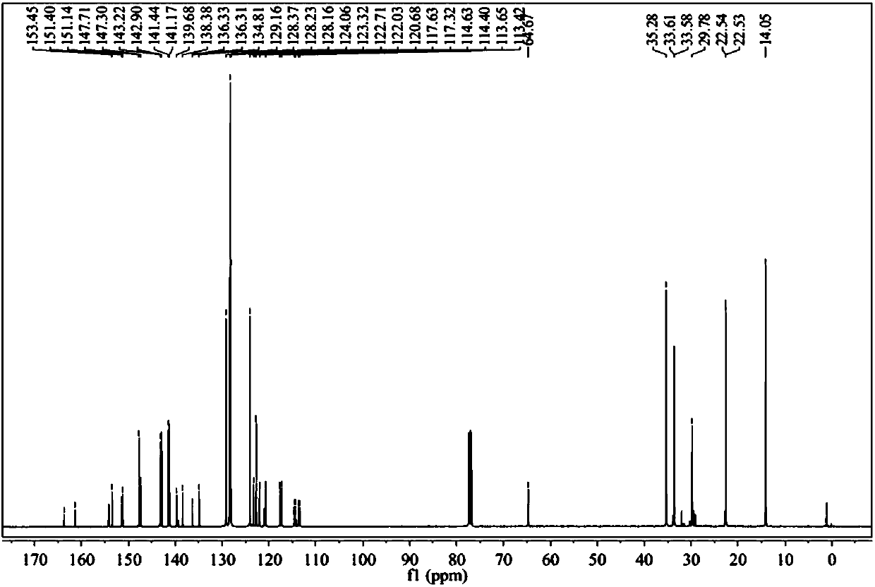
[0042] Example 1 Synthesis of Precursor 1, Precursor 2, and Precursor 3
[0043]
[0044] Step 1: add terebromophthalic acid (12.00g, 36.9mmol) into a 250ml reaction flask, and add 150ml thionyl chloride SOCl 2 , under the condition of nitrogen protection, reflux at 85°C for 12 hours. Thionyl chloride was removed, and butylbenzene (17.1mL, 110.9mmol), aluminum chloride AlCl 3 (7.41g, 55.7mmol), 150mL dichloromethane, react at room temperature for 2 hours. After the reaction, extract with dichloromethane and water, collect the organic phase, dry with anhydrous magnesium sulfate, filter with suction, distill off the solvent to get the solid obtained by chromatographic column purification to obtain intermediate 1 (14.76g, yield 72%);
[0045] The second step: under the protection of light and nitrogen, intermediate 1 (3.0g, 5.4mmol), triphenylamine borate (290.1mg, 1.8mmol), tetrakistriphenylphosphine palladium Pd (PPh 3 ) 4 (103.5mg, 0.09mmol), phase transfer catalyst tet...
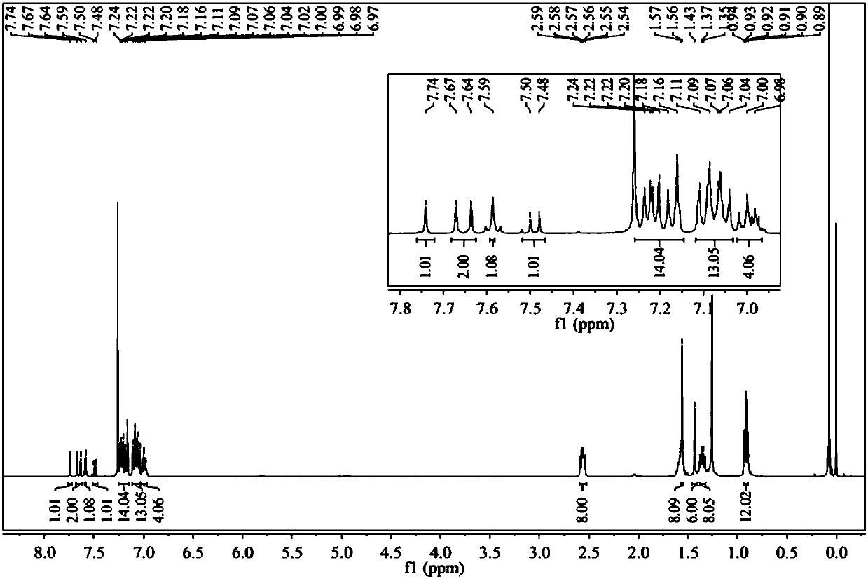
Embodiment 2
[0054] Precursor 1, Precursor 2 and Precursor 3 of Example 1 were used to prepare the following compound A, compound B, compound C, compound D, compound E and compound F.
[0055]
[0056] Wherein, the synthetic route is as follows respectively:
[0057] Reaction route one
[0058]
[0059] Reaction route two
[0060]
[0061] Reaction route three
[0062]
[0063] Reaction route four
[0064]
[0065] Reaction route five
[0066]
[0067] Reaction route six
[0068]
[0069] Since the synthetic methods of Compound A, Compound B, Compound C, Compound D, Compound E, and Compound F are the same, this embodiment takes the synthesis of Compound A as an example, and the specific steps are as follows:
[0070] Step 1, under the conditions of protecting from light and nitrogen, the precursor 1 (300mg, 0.42mmol), 4-fluorophenylboronic acid (117.6mg, 0.84mmol), tetrabutylammonium bromide (65mg, 0.21mmol), four Triphenylphosphinepalladium (24.1mg, 0.02mmol), NaH...
Embodiment 3
[0078] Example 3 Preparation of Organic Laser Devices
[0079] Toluene was used as the solvent, and any one of Compound A, Compound B, Compound C, Compound D, Compound E, and Compound F was used as the light-emitting host to prepare a 20 mg / mL solution. The quartz plate is ultrasonically cleaned, and the organic laser device is prepared by spin coating. The spin coating condition is 2000rpm, and the film thickness is about 100nm. Among them, the emission peaks of the PL spectra of compounds A / B / C / D / E / F are 427nm / 444nm / 465nm / 437nm / 457nm / 472nm, respectively. With the increase of the conjugation length, the PL emission peaks gradually red shift. ASE peaks are at 430nm / 450nm / 468nm / 447nm / 459nm / 474nm; FWHM are 4.5nm / 4.5nm / 5.1nm / 5.1nm / 4.9nm / 6.1nm; ASE threshold is 4.95μJ / cm 2 , 3.49μJ / cm 2 、3.18μJ / cm 2 , 4.12μJ / cm 2 、3.47μJ / cm 2 , 1.97μJ / cm 2 . The optical gain parameters of the light-emitting subject have a certain range of changes with the laser energy, and the maximum gain ...
PUM
 Abstract
Description
Claims
Application Information
 - R&D
- Intellectual Property
- Life Sciences
- Materials
- Tech Scout
- Unparalleled Data Quality
- Higher Quality Content
- 60% Fewer Hallucinations
Browse by: Latest US Patents, China's latest patents, Technical Efficacy Thesaurus, Application Domain, Technology Topic, Popular Technical Reports.
© 2025 PatSnap. All rights reserved.Legal|Privacy policy|Modern Slavery Act Transparency Statement|Sitemap|About US| Contact US: help@patsnap.com