Supercharge Your Innovation With Domain-Expert AI Agents!

A method for growing gete alloy film by thermal atomic layer deposition

An alloy thin film and thermal atom technology, applied in coating, metal material coating process, gaseous chemical plating, etc., can solve the problems of poor thermal stability of precursors, limited application, poor thermal stability, etc., to improve chemical reactivity. , Easy to store and transport, good thermal stability

Active Publication Date: 2019-04-23
JIANGNAN UNIV
View PDF4 Cites 0 Cited by
  • Summary
  • Abstract
  • Description
  • Claims
  • Application Information

AI Technical Summary

Problems solved by technology

Currently, there are only few literature reports on the use of alkyl / amino Ge complexes as ALD precursors to deposit GST
[0009] In 2007, Choi B J et al respectively Ge( i Bu) 4 , Sb( i Pr) 3 , Te( i Pr) 2 As the precursors of Ge, Sb, and Te, GST films were successfully prepared, but only the growth process of Ge films showed the characteristics of saturated growth
In 2007, J.Lee etal selected Ge(N(TMS) 2 ) 4 / Ge(NMe 2 ) 4 , Sb(NMe 2 ) 3 , Te(C 3 h 7 ) 2 GST films were successfully prepared as precursors of Ge, Sb, and Te, but there were high concentrations of Si, C, and N residues
This will inevitably lead to the doping of O and Cl heteroelements in the film, which will affect the performance of the film and the lifetime of the device.
In addition, the GeCl used by Pore et al. 2 (C 4 h 8 o 2 ) The precursor itself has poor thermal stability, and it is easy to form particles on the surface of the film at high temperature, and the generated chloride will cause corrosion to the equipment
Ge(OMe) used by Eom etc. 4 It is difficult to obtain a thin film with the chemical ratio of GST225 from the precursor; Ge(N(TMS) 2 ) 2 Poor thermal stability, etc., limit the application of these Ge precursors

Method used


Image

  • A method for growing gete alloy film by thermal atomic layer deposition
  • A method for growing gete alloy film by thermal atomic layer deposition
  • A method for growing gete alloy film by thermal atomic layer deposition

Examples


Embodiment 1

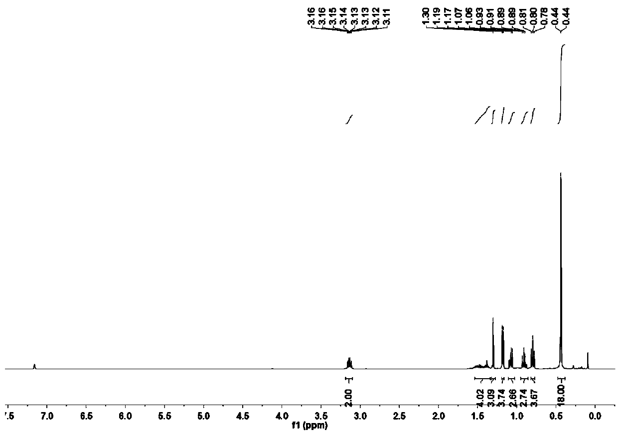
[0087] Embodiment 1: Preparation of (N, N'-di-sec-butyl-methylamidino) (hexamethyldisilazide) Ge (II)

[0088]

[0089] The preparation method of (N, N'-di-sec-butyl-methylamidino) (hexamethyldisilazide) Ge (II) shown in formula III is as follows:

[0090] The 100mL Schlenk bottle was evacuated and replaced with argon three times. Under the protection of argon, N,N'-di-sec-butyl-methylamidine ligand (0.510g, 3mmol) and diethyl ether (15mL) distilled to remove water were added, and the system was Colorless solution. At -78°C, n-butyllithium (1.2 mL, 3 mmol) was added dropwise. Slowly return to room temperature, and continue to stir for 3h, the system is a light yellow solution.

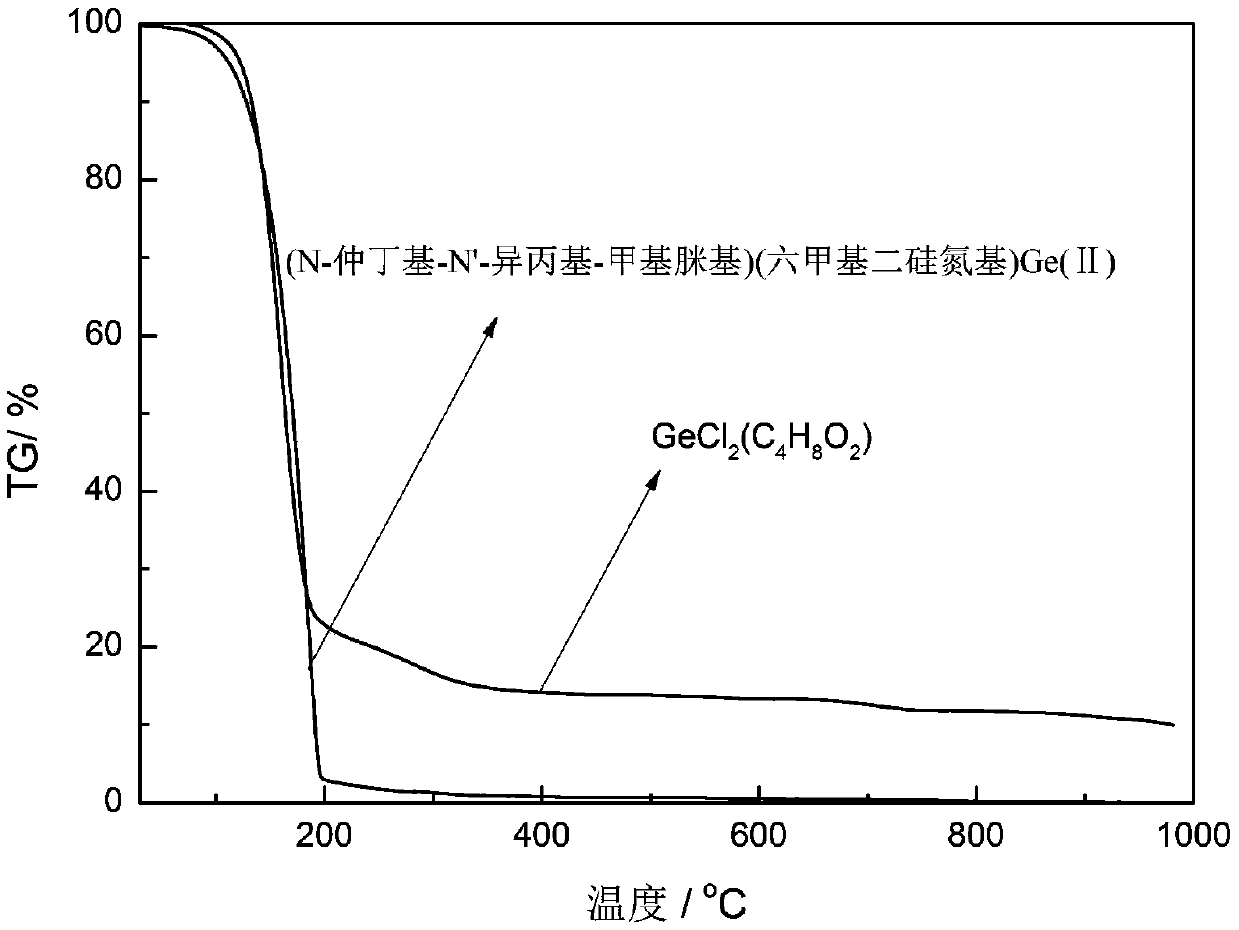
[0091] Another 100 mL Schlenk bottle was evacuated and replaced with argon three times, and germanium dichloride dioxane (0.693 g, 3 mmol) and diethyl ether (10 mL) distilled to remove water were added under the protection of argon. Under the protection of argon gas and at -78°C, the ether soluti...

Embodiment 2

[0096] Example 2: Preparation of GeTe alloy film based on atomic layer deposition

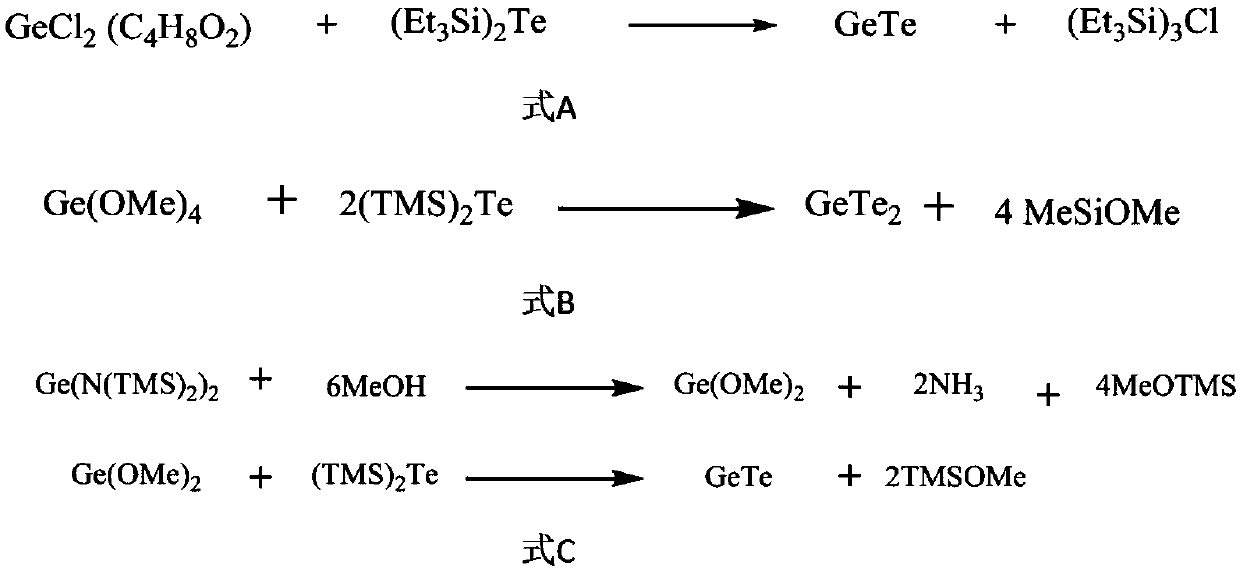
[0097] A kind of (N, N'-di-sec-butyl-methylamidino) (hexamethyldisilazide) Ge (II) as Ge source, see formula III, with N 2 h 4 As reducing agent, with (Et 3 Si) 2 Te is Te source and prepares GeTe alloy thin film atomic layer deposition method, including the following process:

[0098]

[0099] 1) With Si as the substrate, the deposition temperature is 150 °C, and the heating temperature of the Ge source (N,N'-di-sec-butyl-methylamidino) (hexamethyldisilazyl) Ge(II) is 50 ℃, make it vaporized, and use high-purity nitrogen as the carrier gas to pass through the gas phase Ge source (N,N'-di-sec-butyl-methylamidino) (hexamethyldisilazyl) Ge(II), The carrier gas flow rate was 20 sccm. The pulse time is 12s, and the waiting time is 10s;

[0100] 2) Use high-purity nitrogen to clean after completing a Ge source pulse, and the cleaning time is 25s;

[0101] 3) Reducing agent N 2 h 4 The he...

Embodiment 3

[0108] A kind of (N,N'-diisopropyl-n-butylamidino) (hexamethyldisilazide) Ge (II) is Ge source, see has formula IV, with N 2 h 4 As reducing agent, with (Et 3 Si) 2 Te is Te source and prepares GeTe alloy thin film atomic layer deposition method, including the following process:

[0109]

[0110] 1) with SiO 2As the substrate, the deposition temperature is 100°C, and the heating temperature of the Ge source (N,N'-diisopropyl-n-butylamidino)(hexamethyldisilazyl)Ge(II) is 70°C, so that For gasification, high-purity argon was used as the carrier gas, and the gas-phase Ge source (N,N'-diisopropyl-n-butylamidino) (hexamethyldisilazyl) Ge(II) was introduced into the gas phase. The air flow is 50 sccm. The pulse time is 5s, and the waiting time is 20s;

[0111] 2) After completing a Ge source pulse, use high-purity argon to clean, and the cleaning time is 45s;

[0112] 3) The reducing agent MeOH was heated at 70°C to vaporize it. High-purity argon was used as the carrier ga...


PUM

PropertyMeasurementUnit
surface roughnessaaaaaaaaaa
thicknessaaaaaaaaaa
electrical resistivityaaaaaaaaaa

Abstract

The invention discloses a GeTe alloy thin film growing method adopting a hot atom layer deposition technology and belongs to the technical field of semiconductor preparation. According to the GeTe alloy thin film growing method adopting the hot atom layer deposition technology, a Ge source provided with the structure shown in a chemical formula I and a Te source provided with the structure shown in a chemical formula II are adopted, and the Ge source and the Te source are applied into the hot atom layer deposition technology (T-ALD), so that a GeTe deposition layer with a shape-maintaining property is formed on a nanoscale semiconductor device. In addition, an as-deposited GeTe alloy thin film manufactured through the GeTe alloy thin film growing method is higher in resistance, that is, the as-deposited GeTe alloy thin film is higher in purity. According to the GeTe alloy thin film growing method adopting the hot atom layer deposition technology, the resistance of the manufactured GeTe alloy thin film is 1.4*105-4*105 ohm.cm, and root-mean-square roughness of the thin film is 0.7 nm.

Description

technical field [0001] The invention relates to a method for growing a GeTe alloy thin film by thermal atomic layer deposition technology, which belongs to the technical field of semiconductor preparation. Background technique [0002] With the advancement of science and technology, semiconductor technology has been rapidly developed, and the type and manufacturing process technology of memory in microelectronic devices have changed accordingly. Phase change memory (PCRAM) combines the high capacity and low cost of dynamic random access memory (DRAM) and the advantages of high speed, low voltage and low power consumption of static random access memory (SRAM), and has become an internationally recognized next-generation information memory . The core composition of the phase change material is a chalcogenide alloy thin film, among which the GeSbTe225 thin film in the Ge-Sb-Te ternary system is favored for its excellent comprehensive performance. In particular, the preparatio...

Claims


Application Information

Patent Timeline
Patent Type & Authority Patents(China)
IPC IPC(8): C23C16/18C23C16/455
CPCC23C16/18C23C16/455
Inventor 丁玉强杜树雷杜立永
Owner JIANGNAN UNIV
Features
  • R&D
  • Intellectual Property
  • Life Sciences
  • Materials
  • Tech Scout
  • Unparalleled Data Quality
  • Higher Quality Content
  • 60% Fewer Hallucinations
Learn More