Ion implantation doping-based preparation method of hafnium oxide ferroelectric gate

An ion implantation and ferroelectric technology, which is applied in the manufacture of circuits, electrical components, semiconductors/solid-state devices, etc., can solve the problems of demanding heating chamber temperature and reaction gas, increasing experimental costs, process steps, and difficulty in controlling the properties of deposited films, etc. , to achieve the effects of reducing interface effects, controllable performance, and precise depth control

Active Publication Date: 2017-09-08
XIANGTAN UNIV
View PDF4 Cites 13 Cited by
  • Summary
  • Abstract
  • Description
  • Claims
  • Application Information

AI Technical Summary

Problems solved by technology

This technology generally vaporizes the liquid precursor of the required deposition material and deposits it on the substrate. The process temperature requirement for the deposition material with a high boiling point is relatively high, and when depositing two or more materials, in order to make several materials The mixed deposition is uniform, the temperature of the heating chamber and the reaction gas are strict, and the chemical reaction process generally produces by-products, which makes it difficult to control the performance of the deposited film
[0006] (2) When preparing the MFIS structure ferroelectric gate based on ferroelectric hafnium oxide, the process steps are relatively cumbersome. For the preparation of the I layer and the F layer, the same oxide HfO 2 When the HfO 2 After two heat treatments, even two different crystal forms are required, which increases the experimental cost and process steps

Method used


Image

  • Ion implantation doping-based preparation method of hafnium oxide ferroelectric gate
  • Ion implantation doping-based preparation method of hafnium oxide ferroelectric gate

Examples


Embodiment Construction

[0024] The following examples will further illustrate the present invention in conjunction with specific accompanying drawings:

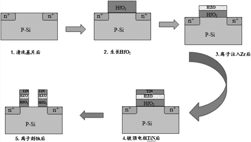
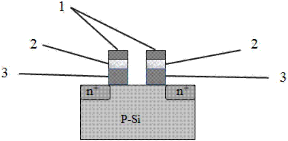
[0025] see figure 1 It is a flow chart of the preparation process of MFIS ferroelectric gate based on ion implantation doping HfO2.

[0026] 1. Take P-Si(100) and clean it with HF to remove the silicon oxide on the surface;

[0027] 2. Use ALD to grow 22nm HfO2 on the silicon wafer as a buffer layer;

[0028] 3. Use ion implantation technology to dope hafnium oxide with Zr to a depth of 11nm, then anneal the ion-implanted sample in oxygen in a rapid annealing furnace, the annealing temperature is 550°C, and the annealing time is 30s;

[0029] 4. Plating 15nm top electrode TiN on the HZO film by CVD, followed by annealing in nitrogen, the annealing temperature is 450°C. Annealing time 30s.

[0030] 5. Finally, perform plasma etching on the MFIS film structure, using argon plasma, chlorine gas plasma, ion beam incident angle 60°, argon ion beam de...


PUM


Abstract

The invention provides an ion implantation doped HfO2 based preparation process of an HfO2 MIFS ferroelectric gate. The preparation process comprises the steps of firstly, cleaning a P-Si or n-Si substrate by a standard cleaning process to remove particles and other pollutants on a Si surface, afterwards depositing an appropriate thickness of HfO2 on a silicon wafer, and performing annealing; secondly, doping HfO2 by an ion implanter, and annealing the doped HfO2; thirdly, depositing a top electrode on the doped HfO2, namely halfnium oxide ferroelectric thin film, and performing rapid thermal treatment on the electrode; and finally, etching an MFIS multi-layer thin film structure to form an MFIS array unit which is matched with the sizes of a source, a drain and a channel by a reactive ion etching method. By the preparation process, the doping concentration of the HfO2 ferroelectric gate thin film can be accurately controlled, and the preparation process is a mature operation process for preparing the thin film relatively simple to prepare and with lower preparation temperature.

Description

technical field [0001] The invention belongs to the field of manufacturing microelectronic devices, and in particular relates to a method for preparing a gate of a transistor-type ferroelectric memory. Background technique [0002] Ferroelectric memory is a new type of non-volatile memory with high read / write speed, wide operating temperature, low power consumption, high radiation resistance, and good fatigue resistance. It has attracted extensive attention from the industry and research circles in recent decades. The market size Steady growth year by year. Ferroelectric memory uses the principle of "0-1" signal corresponding to binary information to realize data storage by using the remanent polarization bistable property of the hysteresis loop of ferroelectric material. At present, the mainstream ferroelectric memories include 1T1C type (1 transistor and 1 ferroelectric capacitor) and 1T type (1 ferroelectric transistor). Among them, the 1T structure ferroelectric memory...

Claims


Application Information

Patent Timeline
Patent Type & Authority Applications(China)
IPC IPC(8): H01L21/28H01L21/265H01L29/792H01L29/423H01L45/00
CPCH01L29/42364H01L29/792H01L21/265H01L21/28158H01L21/28185H10N70/20
Inventor 彭强祥刘巧灵兰杨波廖敏杨琼周益春
Owner XIANGTAN UNIV
Why Eureka
Try Eureka