A kind of back passivation solar cell and preparation method thereof
A solar cell and back electric field technology, applied in circuits, electrical components, photovoltaic power generation, etc., can solve the problems of increased battery series resistance, decreased fill factor, and limited improvement of battery efficiency, achieving increased carrier life, reduced preparation process, The effect of excellent passivation effect
- Summary
- Abstract
- Description
- Claims
- Application Information
AI Technical Summary
Problems solved by technology
Method used
Image
Examples
preparation example Construction
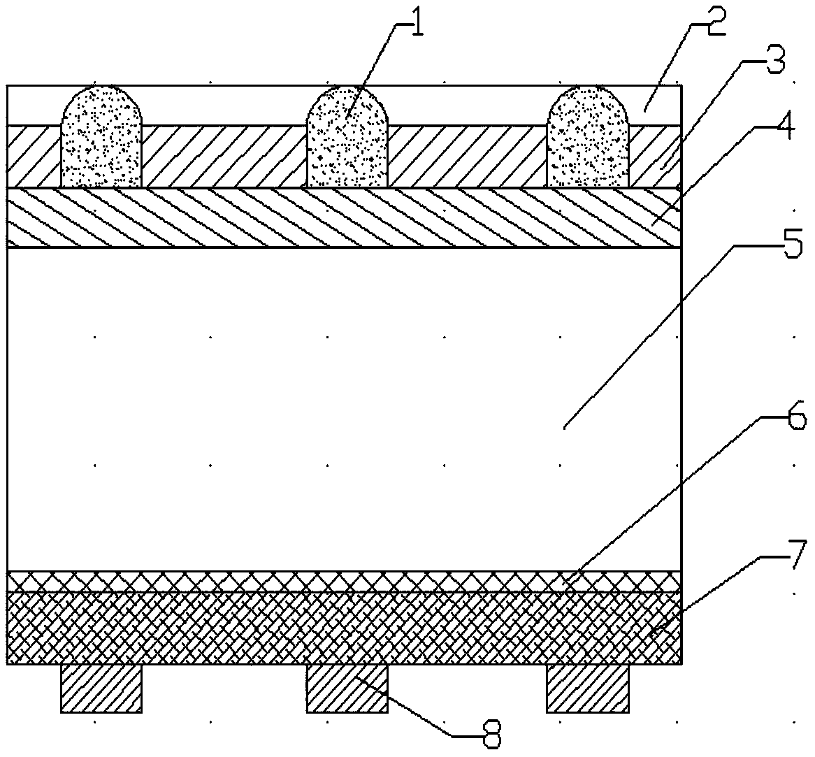
[0028] The present invention also provides a method for preparing a back-passivated solar cell as described above, comprising preparing a front electrode on the light-facing surface of a silicon wafer, and preparing an aluminum layer and a back electrode sequentially on the back-light surface of the silicon wafer; the step of preparing the aluminum layer include:
[0029] S1. Adsorption of alkylaluminum on silicon wafers;
[0030] S2. The silicon wafer adsorbed with alkylaluminum is contacted with hydrogen, and the passivation aluminum layer is obtained by depositing on the backlight surface of the silicon wafer by atomic layer deposition;
[0031] S3. Depositing a layer of metal aluminum on the passivation aluminum layer to obtain a back electric field aluminum layer.
[0032] Specifically, a method for preparing a back passivated solar cell is characterized in that the step of preparing an aluminum layer comprises:
[0033] S1. Alkyl aluminum is adsorbed on the backlight s...
Embodiment 1
[0067] Step 1: Preparation of anti-reflection coating
[0068] The size of the silicon wafer used is: 156mm×156mm, and the thickness is 200μm. After the silicon wafer is textured, diffused and etched, the backlight surface of the silicon wafer is polished. Then, a silicon nitride anti-reflection film layer with a thickness of 80±4 nm and a refractive index of 2.10±0.03 is prepared by PECVD on the light-facing surface of the silicon wafer.
[0069] Step 2: Preparation of passivated aluminum layer
[0070] A passivation aluminum layer with a certain thickness is deposited by microwave electron cyclotron resonance plasma-assisted atomic layer deposition. A passivated aluminum layer is prepared as a reaction cycle, which is divided into four steps: the first step, that is, trimethylaluminum enters the deposition vacuum chamber under the carrying of high-purity argon, and trimethylaluminum is adsorbed on The backlight surface of the silicon wafer is saturated. In this step, the g...
Embodiment 2
[0082] Change the time for depositing the passivation aluminum layer in step 2 in embodiment 1 to 200s, so that the thickness of the passivation aluminum layer becomes 2-3nm, and the rest are the same as in embodiment 1.
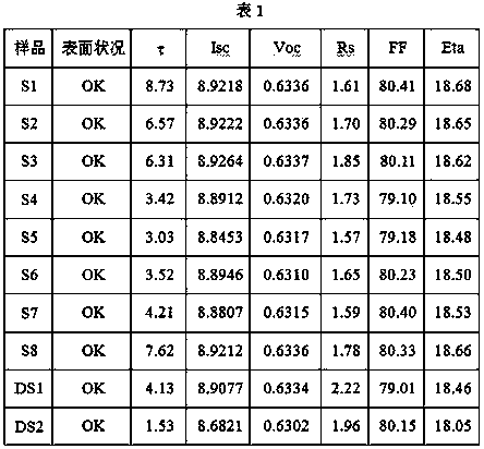
[0083] The solar cell obtained in this example is denoted as S2.
PUM
| Property | Measurement | Unit |
|---|---|---|
| thickness | aaaaa | aaaaa |
| thickness | aaaaa | aaaaa |
| thickness | aaaaa | aaaaa |
Abstract
Description
Claims
Application Information

