N-type surface tunneling oxidation passivation contact manufacturing method for silicon-based solar cell

A solar cell, tunneling oxidation technology, applied in circuits, photovoltaic power generation, electrical components, etc., can solve problems affecting the electrical performance of cells, passivation layer damage, and limited passivation effect, achieving excellent passivation effects and improving Open circuit voltage, effect of reducing interface state density

Inactive Publication Date: 2017-12-12
SHANGHAI SHENZHOU NEW ENERGY DEV
View PDF4 Cites 12 Cited by
  • Summary
  • Abstract
  • Description
  • Claims
  • Application Information

AI Technical Summary

Problems solved by technology

However, these structures have a limited passivation effect on the N-type surface of the cell, and it is inevitable to destroy all or part of the passivation layer in the subsequent process of metallization and current extraction, so that the metal electrode and the silicon wafer directly form a direct contact between the metal electrode and the silicon wafer. Ohmic contact, which leads to great recombination in the metal contact area and affects the electrical properties of the cell

Method used


Image

  • N-type surface tunneling oxidation passivation contact manufacturing method for silicon-based solar cell

Examples


Embodiment 1

[0029] A method for fabricating an N-type surface tunneling oxidation passivation contact of a silicon-based solar cell, specifically adopting the following steps:

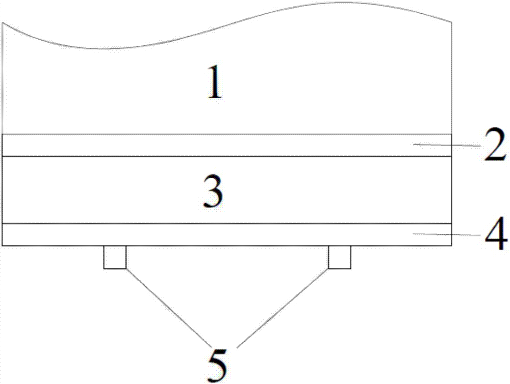
[0030] (1) After the single crystal silicon wafer is etched, textured, polished, diffused and ion implanted, etc., the N-type surface of the single crystal silicon wafer that needs to be tunneled, oxidized, and passivated is cleaned with HF. Removal of SiO on silicon wafer surface 2 , BSG, PSG and other oxide layers;

[0031] (2) Oxidize the surface of the silicon wafer to form an ultra-thin tunnel oxide layer with a thickness of 1 nm. The oxide layer growth method uses concentrated nitric acid to oxidize the surface of the silicon wafer, and the thickness of the oxide layer is controlled by the concentration, temperature and oxidation time of concentrated nitric acid. The concentration of nitric acid is 69%, the temperature is 25°C, and the time is 10 minutes;

[0032] (3) Deposit a thin silicon layer above the...

Embodiment 2

[0038] A method for fabricating an N-type surface tunneling oxidation passivation contact of a silicon-based solar cell, specifically adopting the following steps:

[0039] (1) After etching, texturing, polishing, diffusion, and ion implantation on the single crystal silicon wafer, use the mixed solution of HF and HCl to tunnel the N Clean the surface of the silicon wafer to remove SiO on the surface of the silicon wafer 2 , BSG, PSG and other oxide layers;

[0040](2) Oxidize the surface of the silicon wafer to form an ultra-thin tunnel oxide layer with a thickness of 2nm. Ozone is used to oxidize the surface of the silicon wafer to grow the oxide layer, and the thickness of the oxide layer is controlled by the concentration, temperature and oxidation time of the ozone. The ozone concentration is 50ppm, the temperature is 100°C, and the time is 10 minutes;

[0041] (3) A thin layer of silicon is deposited on the ultra-thin tunneling oxide layer by chemical vapor deposition,...

Embodiment 3

[0046] A method for fabricating an N-type surface tunneling oxidation passivation contact of a silicon-based solar cell, specifically adopting the following steps:

[0047] (1) After the single crystal silicon wafer is etched, textured, polished, diffused and ion implanted, etc., the N-type surface of the single crystal silicon wafer that needs to be tunneled, oxidized, and passivated is cleaned with HF. Removal of SiO on silicon wafer surface 2 , BSG, PSG and other oxide layers;

[0048] (2) Oxidize the surface of the silicon wafer to form an ultra-thin tunnel oxide layer with a thickness of 1.5nm. The way of oxide layer growth is thermal oxidation, and the thickness of the oxide layer is controlled by the oxidation temperature and time. The temperature is 600°C and the time is 20 minutes;

[0049] (3) A thin layer of silicon is deposited on the ultra-thin tunneling oxide layer by chemical vapor deposition, and a low-pressure chemical vapor deposition method is used, and th...


PUM


Abstract

The invention relates to an N-type surface tunneling oxidation passivation contact manufacturing method for a silicon-based solar cell, and the method comprises the following steps: (1), washing the surface of a monocrystalline wafer through a solution after a former operation, and removing a surface oxidation layer; (2), carrying out the oxidation of the surface of the monocrystalline wafer, and forming a superthin tunneling oxidation layer; (3), depositing a silicon thin layer above the superthin tunneling oxidation layer through a chemical vapor deposition method, and completing the phosphor doping of the silicon thin layer; (4), carrying out the oxidizing annealing of the silicon wafer, and further improving the micro-structure and performance of the silicon layer; (5), employing a plasma enhanced chemical vapor deposition method to deposit a silicon nitride passivation antireflection layer above the phosphor-doped silicon thin layer; (6), printing a metal electrode on the surface of the silicon nitride passivation antireflection layer, and completing the manufacturing process. The method can greatly reduce the surface recombination of battery pieces, achieves the excellent passivation effect, and increases the open-circuit voltage. A product has good thermal stability, and there is no need to develop the dedicated low-temperature technology, thereby reducing the cost.

Description

technical field [0001] The invention relates to a method for manufacturing a solar silicon wafer, in particular to a method for manufacturing an N-type surface tunneling oxidation passivation contact of a silicon-based solar cell. Background technique [0002] In order to improve the efficiency of silicon-based solar cells, it is necessary to passivate the surface of the cell well to reduce the recombination of surface defects and increase the open circuit voltage of the cell. The passivation methods currently applied to the N-type surface of cells mainly include full-surface re-doping, selective re-doping, and growth and deposition of silicon oxide, silicon nitride, and silicon oxide / silicon nitride stacks. However, these structures have a limited passivation effect on the N-type surface of the cell, and it is inevitable to destroy all or part of the passivation layer in the subsequent process of metallization and current extraction, so that the metal electrode and the sili...

Claims


Application Information

Patent Timeline
Patent Type & Authority Applications(China)
IPC IPC(8): H01L31/18
CPCH01L31/1868Y02E10/50Y02P70/50
Inventor 钱峥毅汪建强郑飞林佳继张忠卫石磊
Owner SHANGHAI SHENZHOU NEW ENERGY DEV
Why Eureka
Try Eureka