Device and method for preparing in-situ electron microscopy sample by adopting converged femtosecond laser

A femtosecond laser and electron microscope sample technology, used in laser welding equipment, welding equipment, manufacturing tools, etc., can solve the problems that restrict the reliability of in-situ electron microscopes, cannot be widely promoted and applied, and have a low success rate of sample preparation. , to achieve the effect of eliminating the heat-affected zone and the material collapse of the incision and facilitating real-time observation

Pending Publication Date: 2018-03-02
INST OF METAL RESEARCH - CHINESE ACAD OF SCI
View PDF8 Cites 10 Cited by
  • Summary
  • Abstract
  • Description
  • Claims
  • Application Information

AI Technical Summary

Problems solved by technology

The traditional mechanical processing / wire cutting method is still used for the in-situ electron microscopy sample preparation of bulk materials, which has high requirements for the plasticity and machinability of the sample. A series of problems such as pollution, edge effects, and low success rate of sample preparation seriously restrict the efficiency of in-situ electron microscope research and the reliability of results
However, ordinary continuous laser, nanosecond laser or even picosecond laser processing methods, due to their photothermal effect, cause large areas of remelting, recrystallization and oxidation reactions at the edge of material processing, and cannot be used as suitable in-situ electrode samples.
Although the method of preparing in-situ electron microscope samples with focused ion beams can greatly eliminate the edge effect and achieve nanometer-level processing accuracy, the equipment cost is extremely high and the processing efficiency is extremely low, so it cannot be widely promoted and applied.

Method used


Image

  • Device and method for preparing in-situ electron microscopy sample by adopting converged femtosecond laser
  • Device and method for preparing in-situ electron microscopy sample by adopting converged femtosecond laser
  • Device and method for preparing in-situ electron microscopy sample by adopting converged femtosecond laser

Examples


Embodiment 1

[0088] Example 1 Processing of SEM single crystal Ni stretched V-notch sample in situ.

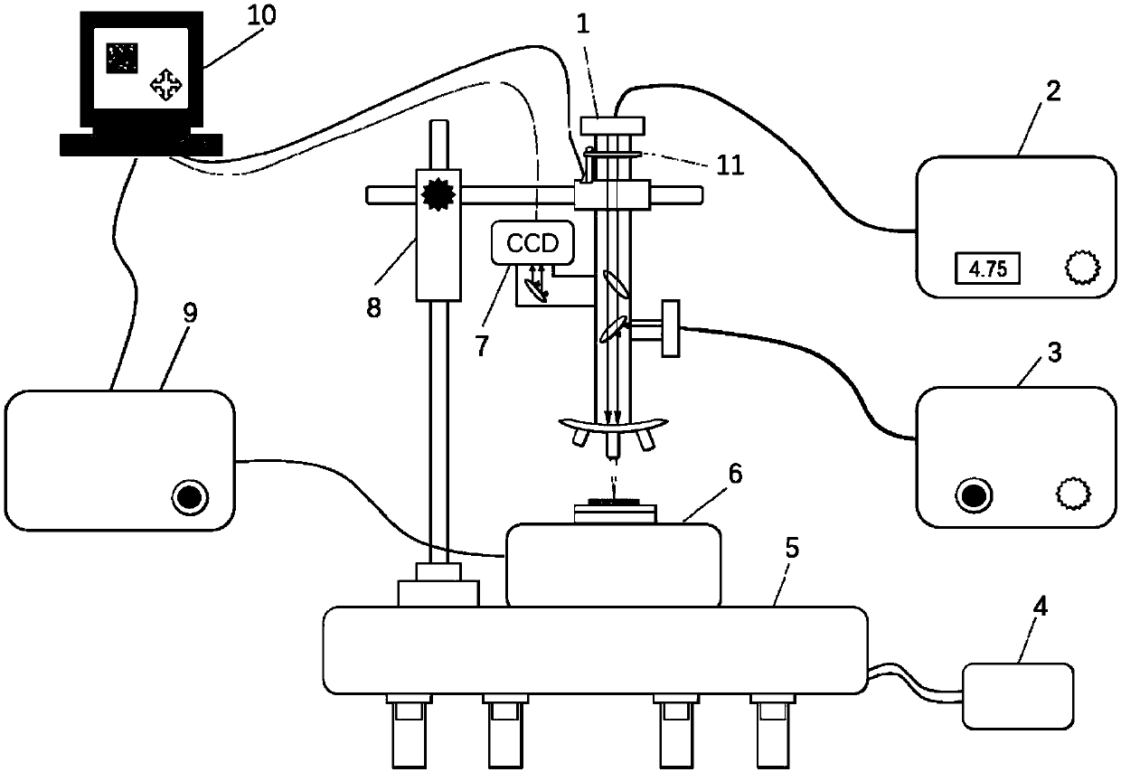
[0089] Such as figure 1 As shown, the equipment used for processing is as described above.

[0090] Processing method: Clamp the single crystal Ni sheet on the sample stage, select an infrared femtosecond laser with a wavelength of 1040nm, and set the power of the laser. By performing the detailed steps of the above-mentioned material processing method, the required strip-shaped scanning in-situ stretching sample with a V-shaped notch can be obtained.

[0091] The results of the examples show that the device of the present invention can quickly and conveniently use the femtosecond laser to finely process various materials, such as metal nickel sheet, transparent quartz glass, etc., with a sample size of less than 10cm×10cm. At the same time, by adjusting the single pulse energy of the femtosecond laser, the spot size, the moving speed of the mechanical platform, etc., an in-situ electron...


PUM


Abstract

The invention relates to the field of laser micro-area machining and preparation of electron microscopy in-situ samples, in particular to a device and method for fine machining and forming an electronmicroscopy sample by utilizing a converged laser. The device comprises a femtosecond laser device and converging scanning system, a sample table mechanical numerical control moving system, a coaxialmicroscopic observation and positioning system, a computer centralized data monitoring and visualization system, a damping system and a protective system. The device can be utilized to quickly and conveniently use femtosecond laser to conduct fine machining such as numerical control cutting and punching on various electron microscopy samples such as a metal sheet, an alumina ceramic block and transparent quartz glass, thereby the in-situ electron microscopy sample with the specific shape and notch can be prepared through the device; combining with an in-situ observation technology through an electron microscope, in-situ observation research such as mechanics, electrics and corrosion behaviors can be conducted on some special tissues and structures; and the device has the advantages of being wide in machining area, and high in precision, having no heat-affected zone and no pollution and the like.

Description

technical field [0001] The invention relates to the field of laser micro-area processing of materials and the field of in-situ electron microscope sample preparation, in particular to a device and method for finely processing prepared samples using a micro-beam femtosecond laser, which can process various materials according to blueprint programming, and can target Different samples are processed in different ways, and there are a variety of sample stages to choose from. Background technique [0002] With the continuous development of laser technology, the performance of lasers has also been continuously improved. The research on the interaction between laser and matter has attracted people's attention, and laser processing technology has also made great progress. [0003] In the early 1990s, with the emergence of broadband tunable laser crystal and self-locking mode technology, femtosecond laser technology has developed by leaps and bounds. The new generation of femtosecon...

Claims


Application Information

Patent Timeline
Patent Type & Authority Applications(China)
IPC IPC(8): B23K26/70B23K26/03
CPCB23K26/032B23K26/702B23K26/707
Inventor 谭军王忠良赵洋靳群邰凯平姜辛
Owner INST OF METAL RESEARCH - CHINESE ACAD OF SCI
Why Eureka
Try Eureka