A wafer-level vacuum packaging method for all-silicon mems based on anodic bonding

A technology of anodic bonding and vacuum packaging, which is applied in the fields of crafts for producing decorative surface effects, decorative arts, microstructure devices, etc. It can solve the problems of large parasitic capacitance of MEMS structures, high processing costs, and low tape-out yields. , to achieve the effect of improving temperature stability, signal-to-noise ratio, and small parasitic capacitance

Active Publication Date: 2019-07-12
BEIJING INST OF AEROSPACE CONTROL DEVICES
View PDF6 Cites 0 Cited by
  • Summary
  • Abstract
  • Description
  • Claims
  • Application Information

AI Technical Summary

Problems solved by technology

However, MEMS wafer-level vacuum packaging using all-silicon bonding uses multiple silicon-silicon bonding processes in the process, which requires high surface roughness, flatness, and cleanliness of the bonding surface, resulting in Tape-out yield is generally low
However, silicon-silicon low-temperature bonding usually uses gold with a thickness of several microns as the solder layer, which causes the problem of high processing costs.
In addition, since silicon dioxide is used as the insulating medium between the silicon substrate, the MEMS structure, and the silicon cover plate, and the thickness of the silicon dioxide prepared by the conventional process is at most 3 microns, the parasitic capacitance between the MEMS structures is very large. Big
MEMS devices mostly use capacitors as sensitive units or drive execution structures. Excessive parasitic capacitance will reduce the sensitivity of MEMS sensors and the drivability of MEMS devices.

Method used


Image

  • A wafer-level vacuum packaging method for all-silicon mems based on anodic bonding
  • A wafer-level vacuum packaging method for all-silicon mems based on anodic bonding
  • A wafer-level vacuum packaging method for all-silicon mems based on anodic bonding

Examples


Embodiment

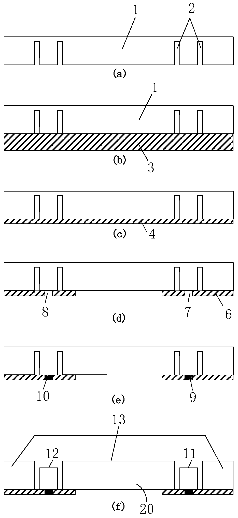
[0050] Such as figure 1 As shown, wherein the processing method of the silicon cover plate starts with the ICP etching (inductively coupled plasma etching) of the low-resistance silicon wafer 1 of the cover plate, and forms the electrode isolation groove 2, as figure 1 (a) shown.

[0051] After ICP etching, the cover plate low-resistance silicon wafer 1 and the cover plate borosilicate glass plate 3 are activated by oxygen plasma for bonding, such as figure 1 (b) shown.

[0052] After bonding, the bonded sheets 1 and 3 are etched in hydrofluoric acid, and the thickness of 3 is reduced to 10-50 microns to form a thin glass layer 4 for the cover plate, such as figure 1 (c) shown.

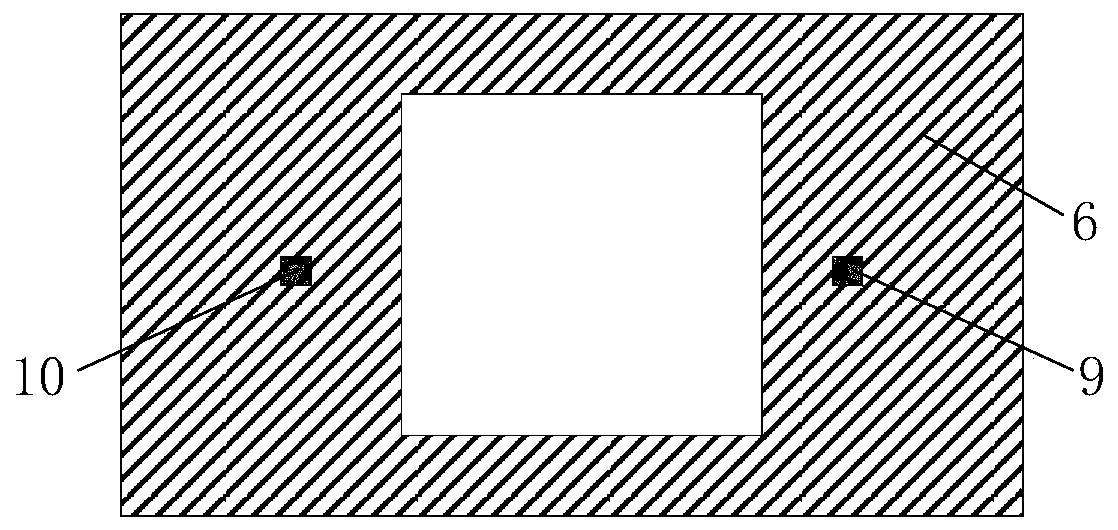
[0053] After photolithography, hydrofluoric acid is used to corrode the thin glass layer 4 of the cover plate to form electrode contact holes 7, 8 and a glass sealing ring 6 on the cover plate.

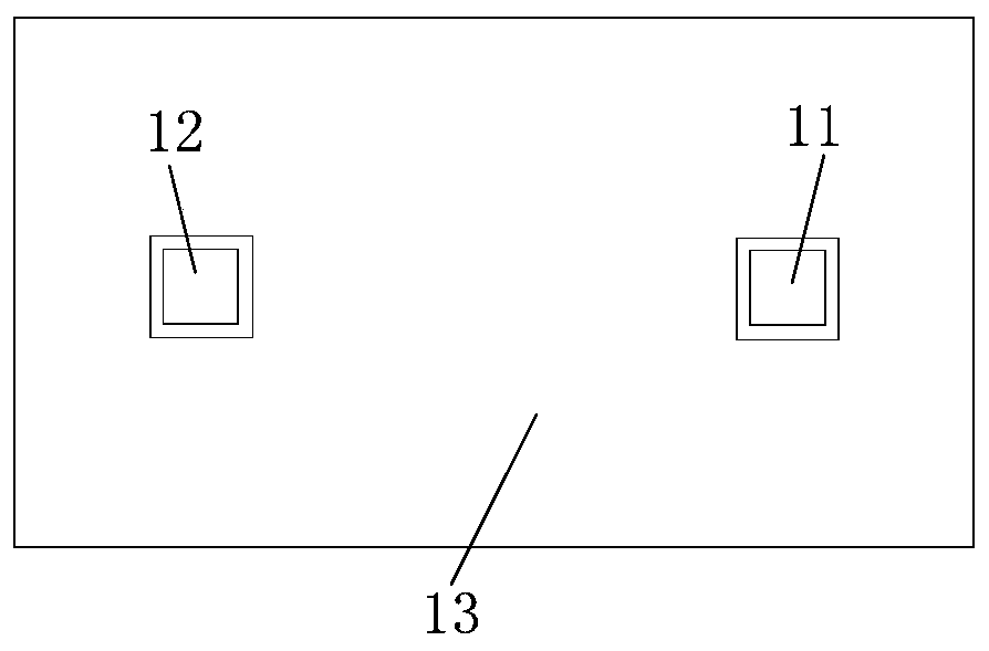
[0054] Through electroplating, evaporation, magnetron sputtering and other processes combined with sub...


PUM

PropertyMeasurementUnit
thicknessaaaaaaaaaa
surface roughnessaaaaaaaaaa
thicknessaaaaaaaaaa

Abstract

The invention discloses a full-silicon MEMS wafer-level vacuum packaging method based on anode bonding; two-time anode bonding is adopted in the MEMS wafer-level vacuum packaging process to realize mechanical and electric signal connection among a cover plate, an MEMS device structure and a substrate and form a pressure controllable MEMS sealing cavity; compared with the existing full-silicon bonding process based on silicon-silicon solder bonding and silicon-silicon fusion bonding, the method in the invention is low in process difficulty and high in rate of finished products; the cover plateglass sheet is thinned to 10-50 microns and the substrate glass sheet is thinned to 10 -50 microns; the thickness of the dielectric layer of the existing full-silicon bonding process is not more than3 microns to the maximum; the thinner dielectric layer is, the larger the introduced parasitic capacitance is; hence, the parasitic capacitance introduced by the method in the invention is small, so that the signal-to-noise ratio output by the MEMS device is improved.

Description

technical field [0001] The invention relates to an all-silicon MEMS wafer-level vacuum packaging method based on anode bonding, which belongs to the technical field of micro-electromechanical systems. Background technique [0002] With the increasing demand for high-performance MEMS sensors in the fields of the Internet of Things, smart devices, and military equipment, the development direction of MEMS technology is developing along the direction of full siliconization, wafer-level packaging, and heterogeneous integration. A typical MEMS device structure generally includes a substrate layer, a MEMS movable structure layer, and a package cover layer. The substrate layer provides mechanical support for the MEMS movable structure. The wafer-level vacuum packaging of MEMS devices is to prepare the third layer of cover plate wafers to seal the MEMS structure between the substrate and the cover plate. The cover plate needs to be used in the cavity. Electrical extraction channels ...

Claims


Application Information

Patent Timeline
Patent Type & Authority Patents(China)
IPC IPC(8): B81C1/00
CPCB81C1/00261B81C1/00269B81C1/00325
Inventor 胡启方李男男杨博邢朝洋梅崴徐宇新庄海涵
Owner BEIJING INST OF AEROSPACE CONTROL DEVICES
Why Eureka
Try Eureka