Film electrode and manufacturing method thereof and application

A thin-film electrode and manufacturing method technology, applied in cable/conductor manufacturing, circuits, conductive materials, etc., can solve the problems of material waste in spin coating process, inability to achieve continuous mass production, etc., and achieve low cost, excellent flexibility, Material saving effect

Active Publication Date: 2018-05-22
NANJING UNIV OF POSTS & TELECOMM
View PDF6 Cites 16 Cited by
  • Summary
  • Abstract
  • Description
  • Claims
  • Application Information

AI Technical Summary

Problems solved by technology

However, the material waste of the spin coating process is serious, and it is impossible to achieve continuous mass production

Method used


Image

  • Film electrode and manufacturing method thereof and application
  • Film electrode and manufacturing method thereof and application
  • Film electrode and manufacturing method thereof and application

Examples


Embodiment 1

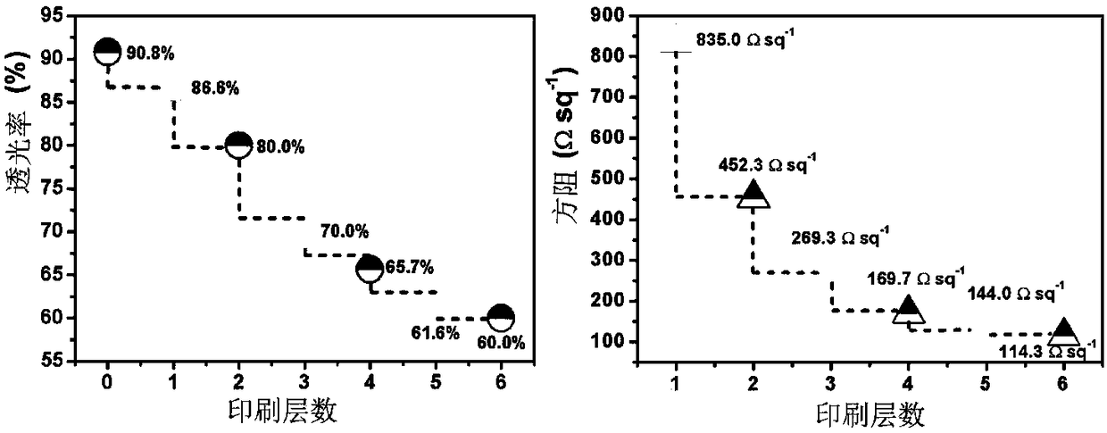
[0025] The polyethylene terephthalate PET substrate was plasma-treated for 10 s and fixed on a screen printing platform. Select a screen mesh number of 300-400 mesh, a film thickness of 6-12 μm, a screen material of stainless steel mesh, and a screen wire diameter of 16-30 μm, and print 1 layer to 6 layers on the treated polyethylene terephthalate substrate. layer of conductive polymer PEDOT-PSS hexagonal mesh. The control grid line width is 50 μm, and the period is 100 μm. Place in a vacuum oven and anneal at 120°C for 30min. figure 1 It can be seen from the figure that as the number of printing layers increases, the square resistance of the flexible electrode decreases, but the light transmittance also decreases, and the optimal number of printing layers is 2 layers.

Embodiment 2

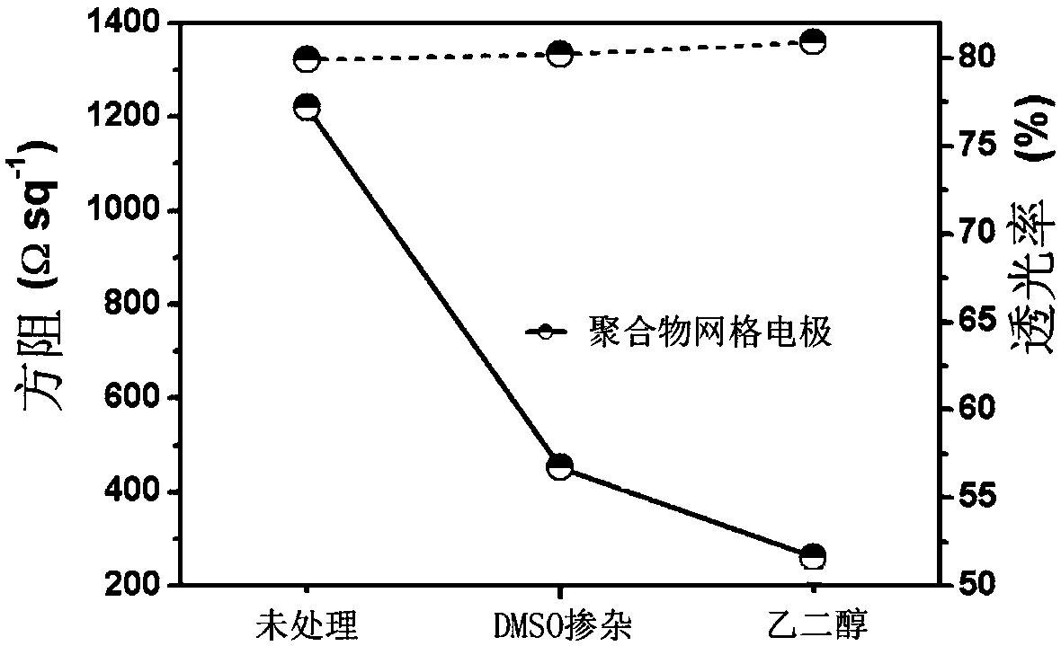
[0027]The polyethylene terephthalate PET substrate was plasma-treated for 10 s and fixed on a screen printing platform. Added 5% dimethylsulfoxide to PEDOT-PSS ink, and stirred it mechanically for 30min. Select a screen mesh number of 300-400 mesh, a film thickness of 6-12 μm, a screen material of stainless steel mesh, and a screen wire diameter of 16-30 μm, and print 2 layers of conductive film on the treated polyethylene terephthalate substrate. Polymer PEDOT / PSS hexagonal mesh. The control grid line width is 50 μm, and the period is 100 μm. Soak in ethylene glycol for 30 minutes, then place in a vacuum oven and anneal at 120°C for 30 minutes. figure 2 It can be seen from the figure that the doping and immersion of the high boiling point solvent has little effect on the light transmittance of the flexible electrode, but effectively reduces the square resistance of the electrode.

Embodiment 3

[0029] The polyethylene terephthalate PET substrate was plasma-treated for 10 s and fixed on a screen printing platform. Added 5% dimethylsulfoxide to PEDOT / SS ink, and stirred it mechanically for 30min. Select a screen mesh number of 300-400 mesh, a film thickness of 6-12 μm, a screen material of stainless steel mesh, and a screen wire diameter of 16-30 μm, and print 2 layers of conductive film on the treated polyethylene terephthalate substrate. Polymer PEDOT:PSS hexagonal mesh. The control grid line width is 50 μm, and the period is 100 μm. Soak in ethylene glycol for 30 minutes, then place in a vacuum oven and anneal at 120°C for 30 minutes. The fabricated hexagonal conductive polymer grid electrodes are shown under the microscope as image 3 shown.


PUM

PropertyMeasurementUnit
widthaaaaaaaaaa
thicknessaaaaaaaaaa
widthaaaaaaaaaa

Abstract

The invention discloses a film electrode and a manufacturing method thereof and application. The electrode is composed of a conductive polymer film and a substrate, and is characterized in that the conductive polymer film has a conductive polymer grid structure; and the conductive polymer can be applied to the substrate such as glass, quartz, fiber, fabric, a plastic film and a polymer film to form the conductive film electrode. Particularly, when a flexible or an extensible transparent substrate is selected, a flexible and transparent film electrode can be manufactured. Patterned grid manufacturing can be realized through a printing method, the process is simple, convenient, economic and efficient, materials are saved, the structure can be controlled, the shape and the size can be adjusted randomly, and more importantly, large-area quick manufacturing can be realized. The electrode can be used as a transparent film electrode to replace an indium tin oxide (ITO) transparent electrode and can be widely used for building a flexible organic light-emitting device, a flexible organic solar cell device, a flexible organic field-effect transistor device or a flexible energy storage device.

Description

technical field [0001] The invention relates to a thin film electrode and its manufacturing method and application, in particular to a conductive polymer grid electrode and its manufacturing method and application, belonging to the field of optoelectronic information materials and applications. Background technique [0002] With the emergence of flexible, portable, low-cost and exquisite wearable electronic products, electrodes as an important part of them not only need excellent photoelectric performance, high flexibility, smooth surface, excellent chemical stability, low-cost fabrication but also need to be feasible. Controlled pattern production and any adjustable size. At present, mainstream thin-film electrodes are made by depositing indium tin oxide (ITO) onto glass or polymer flexible substrates by magnetron sputtering. However, this preparation method requires a high-vacuum environment and complex and expensive equipment. The preparation process is complicated and l...

Claims


Application Information

Patent Timeline
Patent Type & Authority Applications(China)
IPC IPC(8): H01B5/14H01B1/12H01B13/00H01L51/10H01L51/44H01L51/52
CPCH01B1/124H01B5/14H01B13/00H10K10/82H10K30/81H10K50/805Y02E10/549Y02P80/30Y02P70/50
Inventor 赖文勇周璐黄维
Owner NANJING UNIV OF POSTS & TELECOMM
Why Eureka
Try Eureka