Method for preparing large-area single-oriented hexagonal boron nitride two-dimensional atomic crystal

A two-dimensional atomic crystal and hexagonal boron nitride technology, applied in the field of material science, can solve the problems that h-BN research has not been reported yet, and achieve the effects of low cost, good controllability and simple preparation process

Active Publication Date: 2018-06-22
INST OF SEMICONDUCTORS - CHINESE ACAD OF SCI
View PDF3 Cites 6 Cited by
  • Summary
  • Abstract
  • Description
  • Claims
  • Application Information

AI Technical Summary

Problems solved by technology

Based on this, many research groups have prepared large-area graphene single crystals, which fully demonstrates that this solution is very eff

Method used


Image

  • Method for preparing large-area single-oriented hexagonal boron nitride two-dimensional atomic crystal
  • Method for preparing large-area single-oriented hexagonal boron nitride two-dimensional atomic crystal
  • Method for preparing large-area single-oriented hexagonal boron nitride two-dimensional atomic crystal

Examples


Embodiment Construction

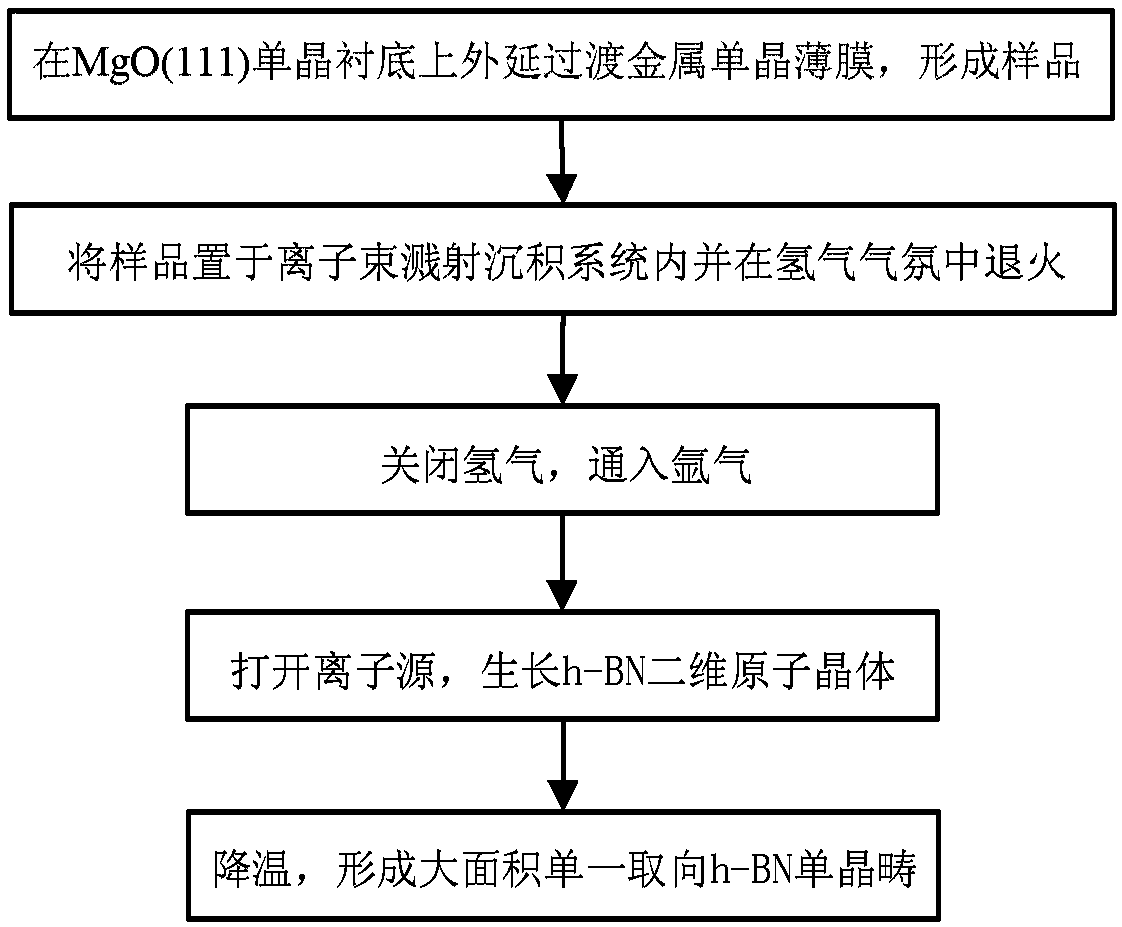
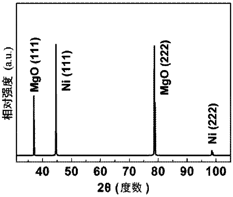
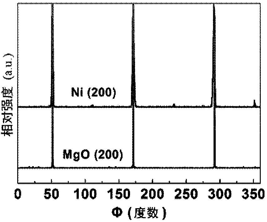
[0020] see figure 1 As shown, the present invention provides a method for preparing a large-area single-orientation hexagonal boron nitride two-dimensional atomic crystal, which includes the following steps:

[0021] Step 1, epitaxially a transition metal single crystal thin film with a predetermined thickness on a magnesium oxide MgO(111) single crystal substrate to form a sample; the MgO(111) single crystal substrate is 100 μm 2 The surface roughness within the range is less than 1.5nm (the present embodiment is 1.0nm); the method of the epitaxial transition metal single crystal thin film is magnetron sputtering method, ion beam sputtering method, molecular beam epitaxy method, thermal evaporation method One or more combination, the preferred epitaxial method is magnetron sputtering (this embodiment is magnetron sputtering); the transition metal single crystal thin film is Ni(111) single crystal thin film or Cu(111 ) single crystal film (this embodiment is Ni(111) single cr...


PUM


Abstract

The invention discloses a method for preparing a large-area single-oriented hexagonal boron nitride two-dimensional atomic crystal. The method comprises the following steps: epitaxially depositing a predetermined thickness of a transition metal single crystal film on a MgO (111) single crystal substrate to form a sample; placing the sample in a chamber of an ion beam sputter deposition system, vacuumizing, heating in a hydrogen atmosphere and annealing in situ; turning off the hydrogen to restore the chamber in the ion beam sputter deposition system to a vacuum environment, and introducing Argon gas to the chamber; bombarding a high-purity boron nitride target placed in the chamber of the ion beam sputtering deposition system with an ion source, so that the sputtered boron and nitrogen atoms are deposited on the surface of the sample to grow and form a hexagonal boron nitride two-dimensional atomic crystal; cooling the hexagonal boron nitride two-dimensional atomic crystal to finally obtain single-oriented hexagonal boron nitride single crystal domains. The method provided by the invention can be used to prepare single-oriented h-BN crystal domains, and has the advantages of simplepreparation process, good controllability, low cost, and non-toxic and harmless by-products, and contributes to achieve the preparation of large-size high-quality h-BN films.

Description

technical field [0001] The invention relates to the technical field of material science, in particular to a method for preparing a large-area single-orientation hexagonal boron nitride two-dimensional atomic crystal. Background technique [0002] Graphene, hexagonal boron nitride (h-BN), MoS 2 The representative two-dimensional atomic crystal material has a unique structure, excellent physical and chemical properties and many potential applications, and has attracted much attention in recent years. Among them, h-BN is an isoelectronic body of graphite, which has a layered structure similar to graphite. Two sets of unequivalent carbon atoms in the graphene two-dimensional atomic crystal are replaced by boron and nitrogen atoms respectively, and the h-BN two-dimensional atomic crystal is obtained. The wide bandgap semiconductor h-BN has many excellent properties, such as excellent electrical insulation, extremely high in-plane elastic modulus, high thermal conductivity, exce...

Claims


Application Information

Patent Timeline
IPC IPC(8): C30B29/40C30B29/64C30B23/02C23C14/02C23C14/06C23C14/34
CPCC23C14/02C23C14/0647C23C14/3442C30B23/02C30B29/403C30B29/64
Inventor 孟军华张兴旺尹志岗吴金良
Owner INST OF SEMICONDUCTORS - CHINESE ACAD OF SCI
Why Eureka
Try Eureka