
A single photon avalanche diode detector structure and manufacturing method thereof

A single-photon avalanche and avalanche diode technology, applied in the field of detectors, can solve the problems that the concentration gradient distribution of four PN junctions is difficult to control, the consistency and repeatability of devices are difficult to guarantee, and the dark count cannot be fundamentally solved. The impurity concentration gradient distribution is simple and controllable, the structure is simple, and the effect of improving the filling rate

Active Publication Date: 2020-01-10
SHANGHAI INTEGRATED CIRCUIT RES & DEV CENT +1
View PDF6 Cites 0 Cited by
  • Summary
  • Abstract
  • Description
  • Claims
  • Application Information

AI Technical Summary

Problems solved by technology

Although it adopts layout technology to reduce dark counts, it cannot fundamentally solve the dark counts caused by defects in STI
To reduce the dark count caused by defects in the STI, only increase the spacing between the STI and the multiplication region, thus increasing the area of ​​the entire unit
In addition, its single-photon avalanche diode structure has four PN junctions along the junction depth direction. Although the time resolution and blue light response can be improved, the implementation process is complicated, and the concentration gradient distribution of the four PN junctions is difficult to control. Device consistency and repeatability are difficult to guarantee

Method used


Image

  • A single photon avalanche diode detector structure and manufacturing method thereof
  • A single photon avalanche diode detector structure and manufacturing method thereof
  • A single photon avalanche diode detector structure and manufacturing method thereof

Examples


Embodiment Construction

[0041] The specific embodiment of the present invention will be further described in detail below in conjunction with the accompanying drawings.

[0042] It should be noted that, in the following specific embodiments, when describing the embodiments of the present invention in detail, in order to clearly show the structure of the present invention for the convenience of description, the structures in the drawings are not drawn according to the general scale, and are drawn Partial magnification, deformation and simplification are included, therefore, it should be avoided to be interpreted as a limitation of the present invention.

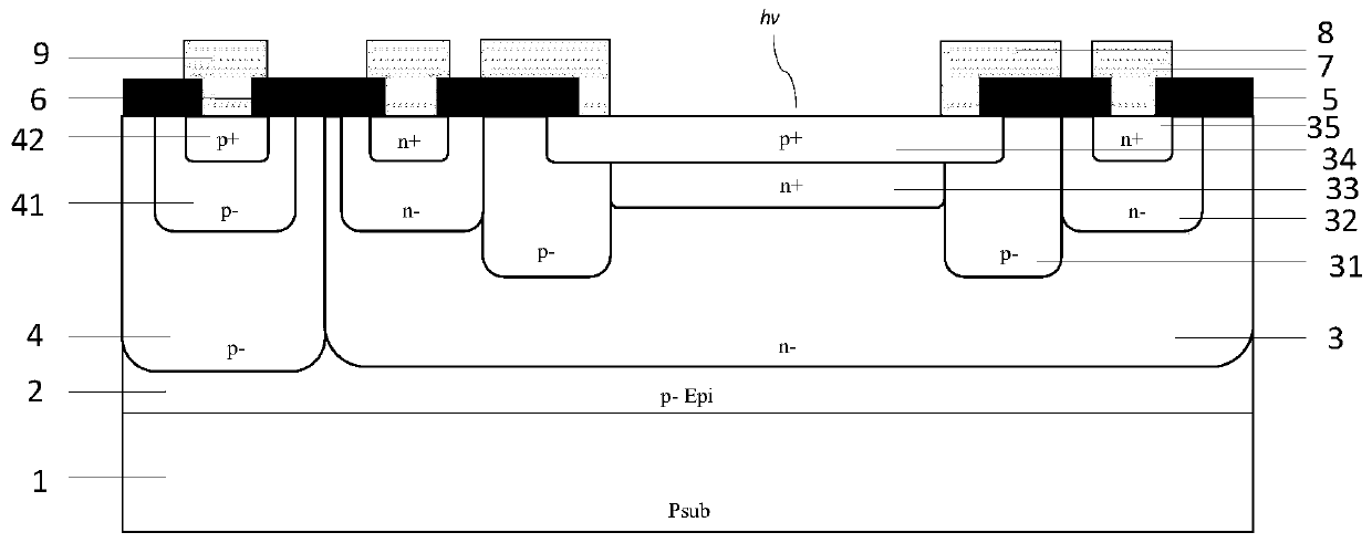
[0043] In the following specific embodiments of the present invention, please refer to figure 1 , figure 1 It is a structural schematic diagram of a single photon avalanche diode detector in a preferred embodiment of the present invention. Such as figure 1 As shown, a single photon avalanche diode detector structure of the present invention includ...


PUM

PropertyMeasurementUnit
thicknessaaaaaaaaaa
thicknessaaaaaaaaaa
thicknessaaaaaaaaaa

Abstract

The invention discloses a single-photon avalanche photoelectric diode detector structure which comprises a P-type silicon substrate, a deep N well and a deep P well, wherein the deep N well and the deep P well are formed in the P-type silicon substrate; an N<+> zone and a P<+> zone for forming a multiplication zone for absorbing photons are formed in the deep N well; a first P well zone and an N well zone for forming an avalanche photoelectric diode structure are formed around the multiplication zone; an anode lead-out end is formed in the N well zone; a cathode lead-out end is formed in the P<+> zone; a second P well zone is formed in the deep P well; a substrate lead-out end is formed in the second P well zone; the surfaces of the deep N well and the deep P well are covered by protectionlayers. The single-photon avalanche photoelectric diode detector structure is simple in structure, only two PN junctions are formed in a vertical direction of a junction depth, a PN junction isolation mode is adopted in a whole unit structure, dark count rates caused by defects of STI can be completely eliminated, the unit area can be greatly reduced, and the filling rate can be increased. The invention further discloses a producing method of the single-photon avalanche photoelectric diode detector structure.

Description

technical field [0001] The present invention relates to the technical field of detectors, in particular to a single photon avalanche diode detector structure and a manufacturing method thereof. Background technique [0002] Single photon detection is a detection method of extremely weak light. The photocurrent intensity of the light detected by it is lower than the thermal noise level (10-14W) of the photodetector itself at room temperature. It is impossible to extract the signal which is buried in the noise. Single-photon detection in high-resolution spectroscopy, non-destructive material analysis, high-speed phenomenon detection, precision analysis, atmospheric pollution measurement, bioluminescence, radiation detection, high-energy physics, astrophotometry, optical time-domain reflectometry, quantum key distribution systems and other fields have a wide range of applications. [0003] The devices currently used in single photon detection mainly include: photomultiplier t...

Claims


Application Information

Patent Timeline
Patent Type & Authority Patents(China)
IPC IPC(8): H01L31/107H01L31/18H01L27/146
CPCH01L27/1463H01L27/14643H01L31/107H01L31/1804Y02P70/50
Inventor 杨冰周伟孙德明
Owner SHANGHAI INTEGRATED CIRCUIT RES & DEV CENT
Learn More