Preparation method and application of segmented copolymer semiconductor nanowire with spiral structure

A technology of block copolymers and helical structures, which is applied in semiconductor/solid-state device manufacturing, semiconductor devices, nanotechnology for materials and surface science, etc., can solve the problems of high difficulty in preparation, control of nanowires, and no gas sensing applications and other problems, to achieve the effect of low requirements on equipment and process conditions, good repeatability, and low detection limit

Active Publication Date: 2018-08-03
HEFEI UNIV OF TECH
View PDF6 Cites 4 Cited by
  • Summary
  • Abstract
  • Description
  • Claims
  • Application Information

AI Technical Summary

Problems solved by technology

The helical structure of the polymer is mainly a special supramolecular structure formed by the self-assembly of the polymer chain induced by the π-π interaction generated by the electrons in the molecule. This structure has a wide range of applications in optical and biological detection. , however, there is no application in gas sensing
[0005] The currently known organic field effect transistors based on block copolymer semiconductor nanowires have not been reported for gas sensing. In addition, the regulation of block copolymer morphology usually requires changing the molecular weight or block ratio of the copolymer. It is difficult to adjust the molecular chain from the polymerization level, and there is no report on the regulation of the morphology (density, diameter) of nanowires only through the preparation conditions of nanowires.

Method used


Image

  • Preparation method and application of segmented copolymer semiconductor nanowire with spiral structure
  • Preparation method and application of segmented copolymer semiconductor nanowire with spiral structure
  • Preparation method and application of segmented copolymer semiconductor nanowire with spiral structure

Examples


Embodiment 1

[0037] The present embodiment prepares PPI (-DMAENBA)-b-P3HT nanowire and organic field effect transistor sensor based on it as follows:

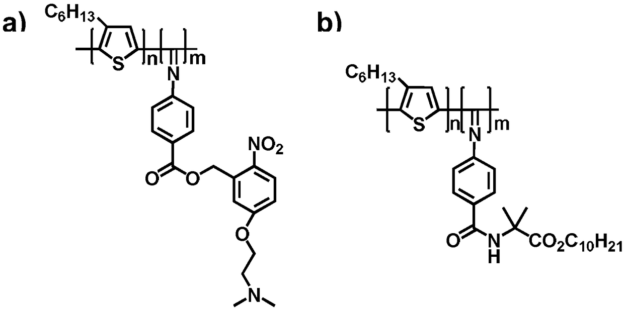
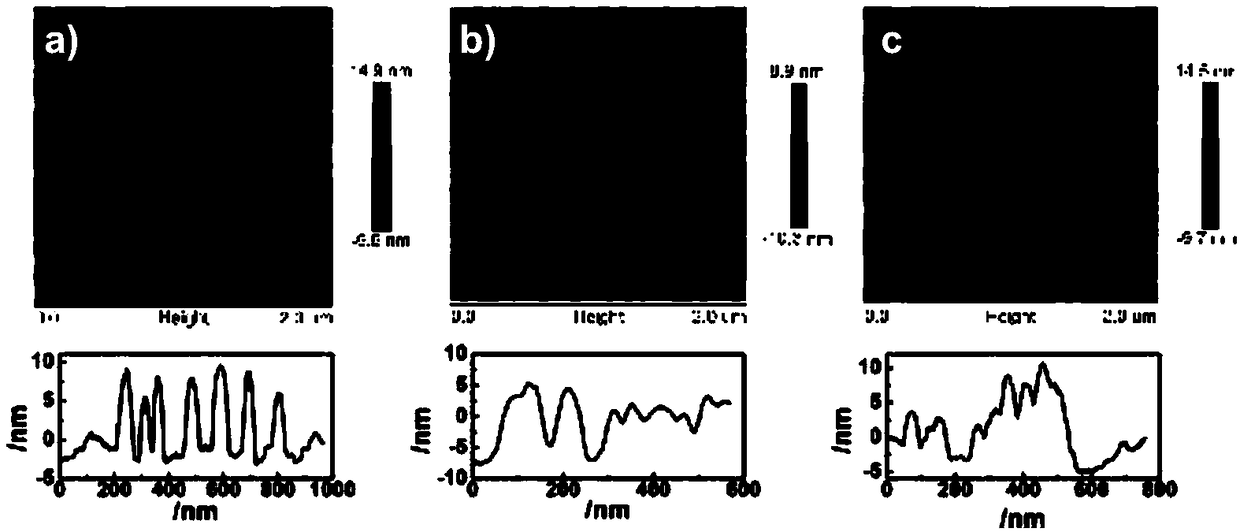
[0038] (1) PPI(-DMAENBA)-b-P3HT is dissolved in o-dichlorobenzene to form a solution A with a concentration of 2mg / mL, and PMMA is dissolved in chlorobenzene to form a solution B with a concentration of 130mg / mL; Mix well with solution B to form a blend solution, in which the mass ratio of PPI(-DMAENBA)-b-P3HT to PMMA is 1:80, or 1:60, or 1:40. The molecular structural formulas of PPI(-DMAENBA)-b-P3HT and PPI-b-P3HT are as follows figure 1shown.

[0039] (2) The n-type silicon wafer is cleaned as a substrate after being heated in a concentrated sulfuric acid-hydrogen peroxide mixed solution; by the spin coating method, the blended solution is spin-coated on the substrate at a speed of 2000 rpm and vacuum-dried at room temperature for 12 hours, thereby On the substrate, a double-layer film with PMMA film as the bottom layer and PPI(-DMAENB...

Embodiment 2

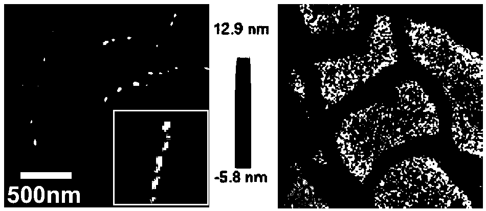
[0048] In this embodiment, helical structure nanowires and organic field effect transistor sensors based on the same method as in Example 1 were prepared, the only difference being that PPI(-DMAENBA)-b-P3HT was replaced with PPI-b-P3HT. The properties of the obtained helical nanowires and sensors are similar to those of Example 1.


PUM

PropertyMeasurementUnit
thicknessaaaaaaaaaa
diameteraaaaaaaaaa

Abstract

The invention discloses preparation method and application of a segmented copolymer semiconductor nanowire with a spiral structure. The preparation method comprises the steps of respectively dissolving a segmented copolymer semiconductor material and a polymer insulation material in solvents, and performing mixing to form a mixed solution; and obtaining the segmented copolymer semiconductor nanowire with the spiral structure and having different density and diameters by controlling a mass ratio of the segmented copolymer semiconductor material and the polymer insulation material. The segmentedcopolymer semiconductor nanowire can be used as a semiconductor layer of an ammonia gas sensor of an organic field-effect transistor, the ammonia gas sensitivity can be improved, the detection limitis reduced, and moreover, the density and the diameter of the nanowire can be changed by changing a preparation process condition. The segmented copolymer semiconductor nanowire with the spiral structure is initially prepared by a mixing method and is used for ammonia gas sensing, and relatively high sensitivity is obtained.

Description

technical field [0001] The invention relates to the field of organic semiconductor nanostructures and devices, in particular to a method for preparing a helical-structured block copolymer semiconductor nanowire and its application. Background technique [0002] Ammonia (NH3), as an important chemical raw material, is widely used in industrial production, food storage, safety requirements and other fields. Due to the strong toxicity of ammonia gas, when the human body is exposed to a low-concentration ammonia environment, it can produce poisoning symptoms such as edema in the respiratory tract and gastric mucosa. Therefore, it is very important to prepare an ammonia sensor with high sensitivity, low detection limit and stable performance. [0003] Conjugated polymer organic field effect transistors have received extensive attention and research in recent years due to their potential advantages such as large-area solution processing, flexible devices, and low cost. The organ...

Claims


Application Information

Patent Timeline
Patent Type & Authority Applications(China)
IPC IPC(8): H01L51/05H01L51/30H01L51/40G01N27/414B82Y40/00B82Y30/00
CPCG01N27/4141B82Y30/00B82Y40/00H10K71/12H10K85/151H10K10/462
Inventor 邱龙臻魏诗语田丰收王晓鸿陆红波
Owner HEFEI UNIV OF TECH
Why Eureka
Try Eureka