Semiconductor composite heterojunction photoelectrode and manufacturing method thereof
A composite heterojunction and photoelectrode technology, which is applied in photovoltaic power generation, photosensitive equipment, circuits, etc., can solve the problems that restrict the development of the field of photo-splitting water, low utilization efficiency, and complicated preparation methods, so as to improve the efficiency of photo-splitting water , Utilization efficiency improvement, the effect of promoting chemical reaction
- Summary
- Abstract
- Description
- Claims
- Application Information
AI Technical Summary
Problems solved by technology
Method used
Image

Examples
Embodiment 1
[0035] (1) Using FTO as the conductive substrate, the conductive substrate was ultrasonically cleaned in an ultrasonic machine for 30 minutes in the order of acetone, absolute ethanol and deionized water.
[0036] Dissolve 1.6169g of bismuth nitrate pentahydrate and 1.2808g of anhydrous citric acid in 10mL of nitric acid (concentration: 23.3%), and keep stirring until uniformly mixed. 0.39 g of ammonium metavanadate was dissolved in the above solution and stirred. After the solution was completely dissolved, 0.4 g of polyvinyl alcohol (PVA) was added and stirred for 5 hours to obtain a transparent blue solution.
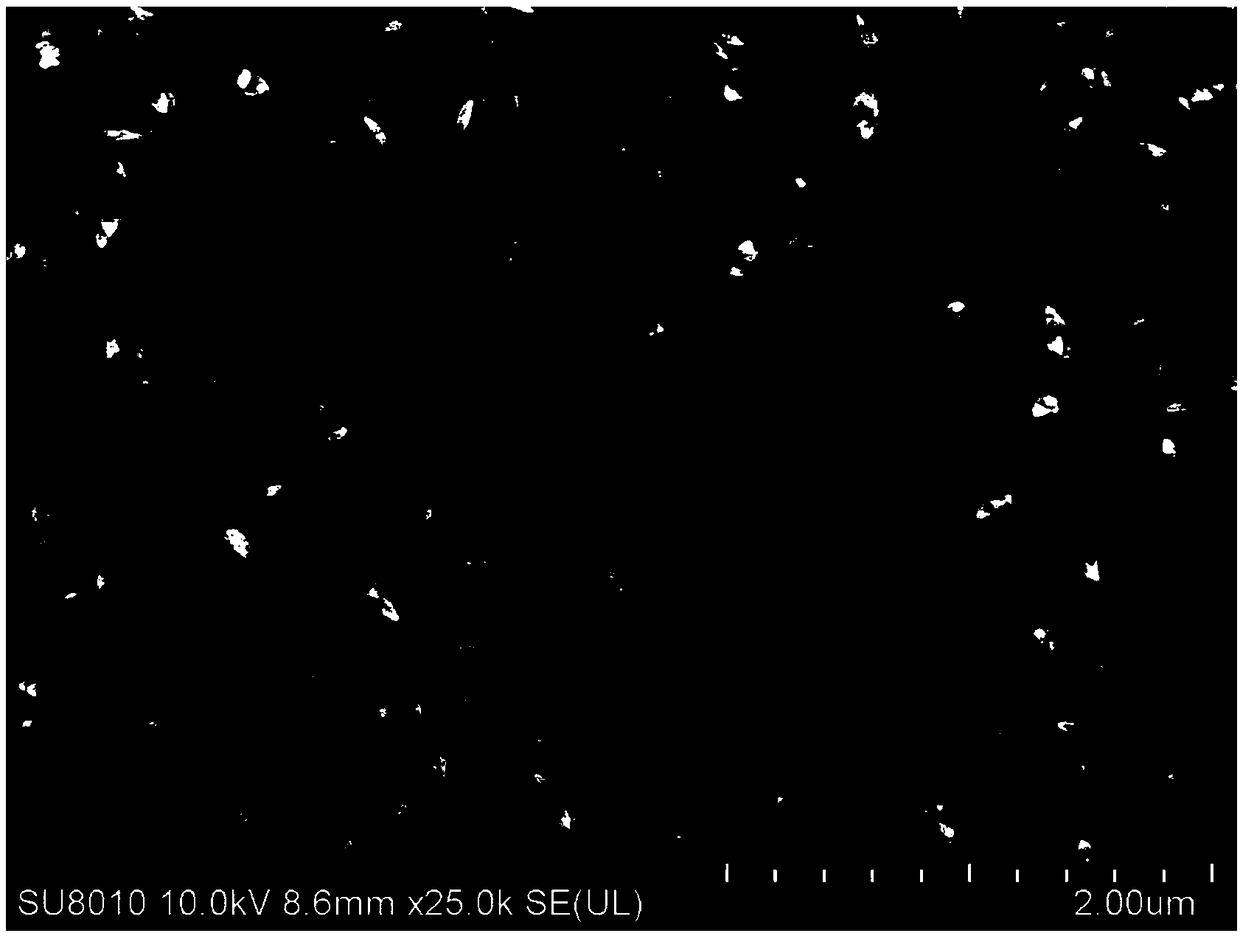
[0037] Put the cleaned conductive substrate on the spin coater, use a pipette gun to take an appropriate amount of transparent blue solution and drop it on the conductive substrate, and obtain a bismuth vanadate film by spin coating. The spin coating speed is 4000 rpm. The process loops 5 times. The spin-coated conductive substrate was calcined in an annealing furna...
Embodiment 2
[0044] Prepare BiVO according to the method of Example 1 steps (1)-(3) 4 / CuO / TiO 2 Composite electrode, the difference is that in step (3), TiO with different cycle numbers is deposited by controlled ALD technology 2 program to obtain TiO with different thicknesses 2 , so that the TiO in step (3) 2 The thickness is 1 nm.
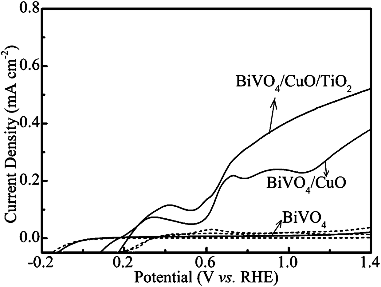
[0045] The above-prepared photoelectrodes were assembled into photoelectrochemical cells, and then water was split under different voltages. Under the voltage of 1.23V, the photocurrent of the photoelectrode prepared by the method of this embodiment can reach 0.412mA / cm 2 ; and with BiVO 4 / CuO sample as the working electrode photocurrent is only 0.299mA / cm 2 .
Embodiment 3
[0047] Prepare BiVO according to the method of Example 1 steps (1)-(3) 4 / CuO / TiO 2 For the composite electrode, the difference is that the reaction time in the water bath in step (2) is 15 minutes, so that the reaction time of the step of converting ZnO into CuO is different, and a CuO petal-shaped morphology with a different density from Example 1 is obtained.
[0048] The above-prepared photoelectrodes were assembled into photoelectrochemical cells, and then water was split under different voltages. Under the voltage of 1.23V, the photocurrent of the photoelectrode prepared by the method of this embodiment can reach 0.38mA / cm 2 ; and with BiVO 4 / CuO sample as the working electrode photocurrent is only 0.2mA / cm 2 .
PUM
| Property | Measurement | Unit |
|---|---|---|
| thickness | aaaaa | aaaaa |
| thickness | aaaaa | aaaaa |
| photocurrent | aaaaa | aaaaa |
Abstract
Description
Claims
Application Information
 - R&D
- Intellectual Property
- Life Sciences
- Materials
- Tech Scout
- Unparalleled Data Quality
- Higher Quality Content
- 60% Fewer Hallucinations
Browse by: Latest US Patents, China's latest patents, Technical Efficacy Thesaurus, Application Domain, Technology Topic, Popular Technical Reports.
© 2025 PatSnap. All rights reserved.Legal|Privacy policy|Modern Slavery Act Transparency Statement|Sitemap|About US| Contact US: help@patsnap.com