Efficient and stable silicon-based photo-splitting water hydrogen production electrode and its preparation method and application
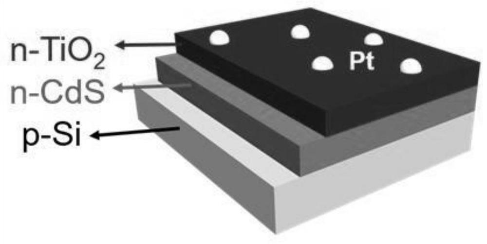
A photo-splitting water hydrogen production and stable technology, applied in the direction of electrodes, electrolysis components, electrolysis process, etc., can solve the problems of insufficient photo-generated voltage and instability of single crystal silicon photocathode, and achieve the improvement of photo-splitting water hydrogen production activity, enhanced The effect of stability and simple operation process
- Summary
- Abstract
- Description
- Claims
- Application Information
AI Technical Summary
Problems solved by technology
Method used
Image
Examples
Embodiment 1
[0046] (1) Silicon wafer cleaning
[0047] Cut the p-Si finished product into several small squares of 2cm×2cm.
[0048] a) Piranha solution at 85°C (V 浓硫酸 :V 浓过氧化氢 =3:1) for 10min, rinse with deionized water, N 2 Blow dry to remove organic pollutants on the surface of the Si wafer;
[0049] b) Soak the silicon wafer in an aqueous solution of 1% HF by volume in turn for 2 minutes, rinse with deionized water, N 2 Blow dry, this step can remove SiO 2 and accompanying metal;
[0050] c) In order to further thoroughly remove the organic matter and heavy metals on the Si sheet, soak the Si sheet in the RCAII solution at 75°C (V 浓过氧化氢 :V 浓盐酸 :V 水 =1:1:6) for 15min, rinse with deionized water, N 2 Blow dry and set aside.
[0051] (2) Preparation of cadmium sulfide layer
[0052] a) Precursor solution preparation: take 0.625g cadmium sulfate (CdSO 4 ), dissolved in 20mL of deionized water, that is, the concentration of cadmium sulfate is 0.015mol / L, 1.1418g thiourea is dis...
Embodiment 2
[0060] (1) Silicon wafer cleaning
[0061] a) with embodiment 1;
[0062] b) Soak the silicon wafer in 1% HF solution with a volume concentration of 1% for 1 min, rinse with deionized water, N 2 Blow dry, this step can remove SiO 2 and accompanying metal.
[0063] c) with embodiment 1;
[0064] (2) the preparation of cadmium sulfide layer is with embodiment 1;
[0065] (3) The preparation of protective layer is with embodiment 1;
[0066] (4) The deposition of platinum auxiliary agent is the same as that in Example 1.
Embodiment 3
[0068] (1) Silicon wafer cleaning
[0069]a) with embodiment 1;
[0070] b) Soak the silicon wafers in 1% HF solution with a volume concentration of 1% for 3 minutes, rinse with deionized water, N 2 Blow dry, this step can remove SiO 2 and accompanying metal.
[0071] c) with embodiment 1;
[0072] (2) the preparation of cadmium sulfide layer is with embodiment 1;
[0073] (3) The preparation of protective layer is with embodiment 1;
[0074] (4) The deposition of platinum auxiliary agent is the same as that in Example 1.
PUM
| Property | Measurement | Unit |
|---|---|---|
| thickness | aaaaa | aaaaa |
Abstract
Description
Claims
Application Information


