Organic thin film transistor containing dual dielectric layers and fabrication method of organic thin film transistor

An organic thin film and transistor technology, applied in the field of organic thin film transistors and their preparation, can solve problems such as thermal and electrical instability of transistors, and achieve the effects of improving thermal stability, reducing dark current, and improving on-off ratio.

Pending Publication Date: 2018-08-17
PEKING UNIV SHENZHEN GRADUATE SCHOOL
View PDF3 Cites 4 Cited by
  • Summary
  • Abstract
  • Description
  • Claims
  • Application Information

AI Technical Summary

Problems solved by technology

[0005] In view of the above deficiencies in the prior art, the object of the present invention is to provide an organic thin film transistor containing a double-layer dielectric layer and its preparation method, aiming to solve the problems of thermal and electrical instability in existing transistors

Method used


Image

  • Organic thin film transistor containing dual dielectric layers and fabrication method of organic thin film transistor
  • Organic thin film transistor containing dual dielectric layers and fabrication method of organic thin film transistor
  • Organic thin film transistor containing dual dielectric layers and fabrication method of organic thin film transistor

Examples


preparation example Construction

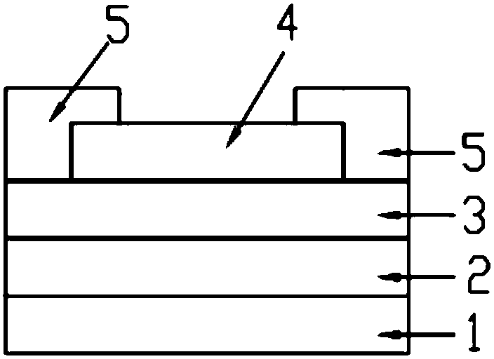
[0071] The present invention also provides a preferred embodiment of the above-mentioned method for preparing an organic thin film transistor, including:

[0072] Step A, making a first dielectric layer on the gate substrate;

[0073] Step B, making a fluorine-containing polyimide film on the first dielectric layer;

[0074] Step C, making an organic semiconductor layer on the fluorine-containing polyimide film;

[0075] Step D, making an electrode on the fluorine-containing polyimide film with an organic semiconductor layer, both the organic semiconductor layer and the fluorine-containing polyimide film are overlapped with the electrode, and the organic thin film transistor is fabricated.

[0076] For the first dielectric layer, when selecting inorganic dielectric materials to make the dielectric layer, magnetron sputtering can be used; when polymer materials are used to make the dielectric layer, thermal evaporation, scrape coating or spin coating can be used. Made by pain...

Embodiment 1

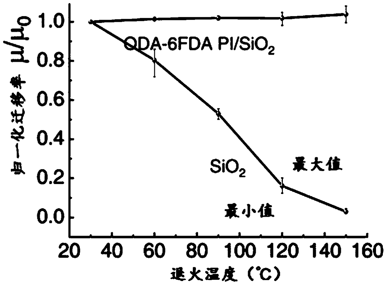
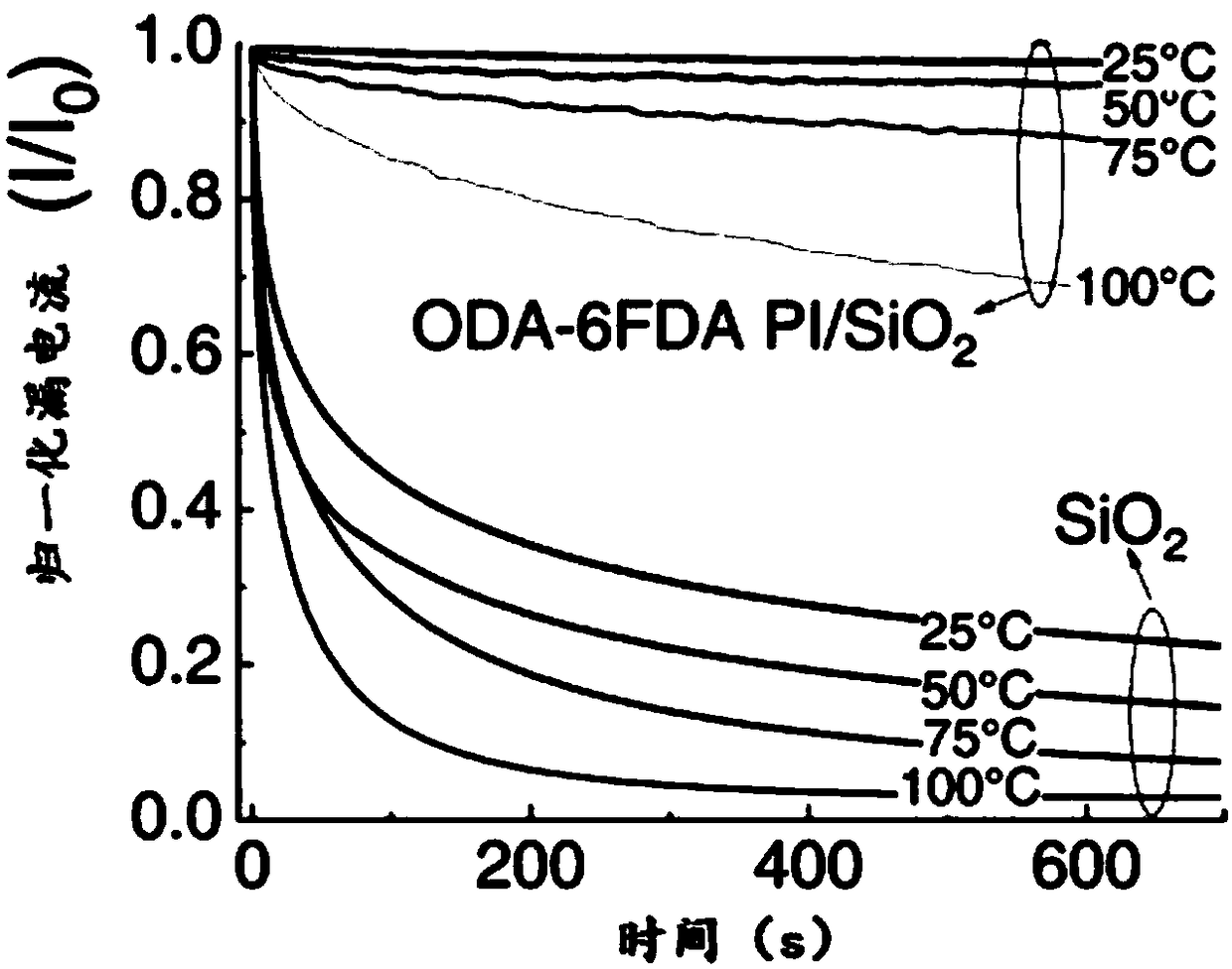
[0082] Embodiment 1 is made to contain ODA-6FDA PI / SiO 2 Organic Thin Film Transistor with Double Dielectric Layer

[0083] (1) Use n-type doped polysilicon Si as the gate substrate, and form a layer of 300nm SiO on the Si substrate by thermal oxidation 2 as the first dielectric layer.

[0084] (2) Then cleaning, the cleaning steps are as follows: the gate substrate formed with the first layer of dielectric layer is immersed in deionized water, acetone and isopropanol successively, each ultrasonic 15 minutes, and use N 2 Blow dry, UV ozone treatment for 30min.

[0085] (3) ODA (4,4'-diaminodiphenyl ether) and 6FDA (4,4'-(hexafluoroisopropylene) diphthalic anhydride) were added to NMP successively in a molar ratio of 1:1, and the Stir in a water bath for 24h to form a solution with a mass fraction of ODA-6FDA PAA (fluorine-containing polyamic acid) of 10%, then dilute it to a mass fraction of 3.33% with a DMF solvent, and spin-coat the obtained dilution on the first dielectr...


PUM

PropertyMeasurementUnit
thicknessaaaaaaaaaa
thicknessaaaaaaaaaa

Abstract

The invention discloses an organic thin film transistor containing dual dielectric layers and a fabrication method of the organic thin film transistor. The organic thin film transistor sequentially comprises a gate substrate, a first dielectric layer, a second dielectric layer, an organic semiconductor layer and an electrode from bottom to top, wherein the material of the first dielectric layer isan inorganic dielectric material or a polymer material with a dielectric constant larger than 5, the material of the second dielectric layer is fluorine-containing polyimide, and the organic semiconductor layer and the second dielectric layer both are in overlapped joint with the electrode. The probability of charge trapped by a pit is reduced by hydrophobicity of the fluorine-containing polyimide at an upper layer, and meanwhile, the thermal stability of the transistor is improved by thermal expansion coefficient and favorable extensibility which are relatively matched of the fluorine-containing polyimide; the dielectric layer at a lower layer is used for reducing a dark current of the device, and positive drift of a threshold voltage is prevented; and by designing dual dielectric layers, the thermal stability and the electrical stability of the organic thin film transistor are improved.

Description

technical field [0001] The invention relates to the technical field of transistors, in particular to an organic thin film transistor containing double dielectric layers and a preparation method thereof. Background technique [0002] Organic thin-film transistors (OTFT), compared with transistors made of inorganic materials, have better mechanical flexibility and manufacturing convenience, and have greatly improved carrier mobility, operating voltage and manufacturing methods, and can Applications such as large-area flexible displays, memory, radio frequency identification tags and electronic components such as chemical or biological sensors. [0003] However, organic thin film transistors suffer from serious thermal and electrical instability defects in practical applications. Thermal instability manifests itself as degradation of the device and can be attributed to: changes in crystal structure or morphology, or thermally induced mechanical stress from a large thermal expa...

Claims


Application Information

Patent Timeline
Patent Type & Authority Applications(China)
IPC IPC(8): H01L51/05H01L51/40
CPCH10K10/474H10K10/476
Inventor 孟鸿魏潇赟李爱源曹菊鹏朱淼
Owner PEKING UNIV SHENZHEN GRADUATE SCHOOL
Why Eureka
Try Eureka