

Epitaxial wafer manufacturing method and epitaxial wafer
A manufacturing method and wafer technology, applied in semiconductor/solid-state device manufacturing, electrical components, circuits, etc., can solve problems such as the occurrence of particles, the reduction of oxygen precipitates, and the increase of workload.
- Summary
- Abstract
- Description
- Claims
- Application Information
AI Technical Summary
Problems solved by technology
Method used
Image

Examples
Embodiment 1
[0056] In order to examine the effect of nitrogen doping, the following two experiments were carried out. The conditions for single crystal growth were as follows: 50 kg of high-purity polycrystalline silicon was melted in a quartz crucible, boron was used as a dopant, and the pulling speed of a single crystal with a diameter of 150 mm and a crystal orientation was set to 0.6 mm / min.
[0057] First of all, in the first step, in order to highlight the effect of nitrogen addition, when the single crystal grows to the bottom right 300mm stage, nitrogen flow is put into the furnace at 10L / min to continue growing in this state, and increase the nitrogen in the single crystal. Next, in order to easily estimate the amount of nitrogen doping, nitrogen is not added in the form of gas during pulling, but the silicon wafer with a clear amount of nitrogen to form the nitride film is melted together with high-purity polysilicon as the raw material to grow nitrogen. Doping amount is 10 12...
Embodiment 2
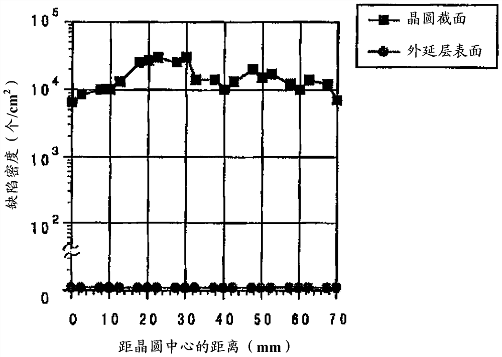
[0062] In Example 1, for slave doping with 10 14 atoms / cm 3 The epitaxial layer with a thickness of about 5 μm was formed at a deposition temperature of 1150° C. on a wafer obtained from a single crystal of nitrogen. The obtained wafer test piece was subjected to selective etching for 5 minutes using a photoetching solution, and the defect density on the surface of the epitaxial layer and the defect density on the cross section were measured with an optical microscope.
[0063] image 3 , shows the results of density measurement of surface and cross-sectional defects at positions in the direction from the center of the test piece toward the outer periphery. According to this, it can be seen that after the epitaxial layer is formed on the wafer made of the single crystal doped with nitrogen, the cross section of the single crystal in the lower layer has been observed 10 4 piece / cm 2 It has been confirmed that oxygen precipitates do not easily disappear even when a high-temp...
Embodiment 3
[0065] Taking two types of p-type wafer substrates with a resistivity of 10Ωcm or 0.008Ωcm, high resistance or low resistance, respectively, a single crystal undoped with nitrogen and doped with 10 12 、10 13 or 10 14 atoms / cm 3 Eight kinds of single crystals of nitrogen were cut out from wafer substrates, and an epitaxial layer with a thickness of 5 μm was formed at a deposition temperature of 1150° C. to form an epitaxial wafer.
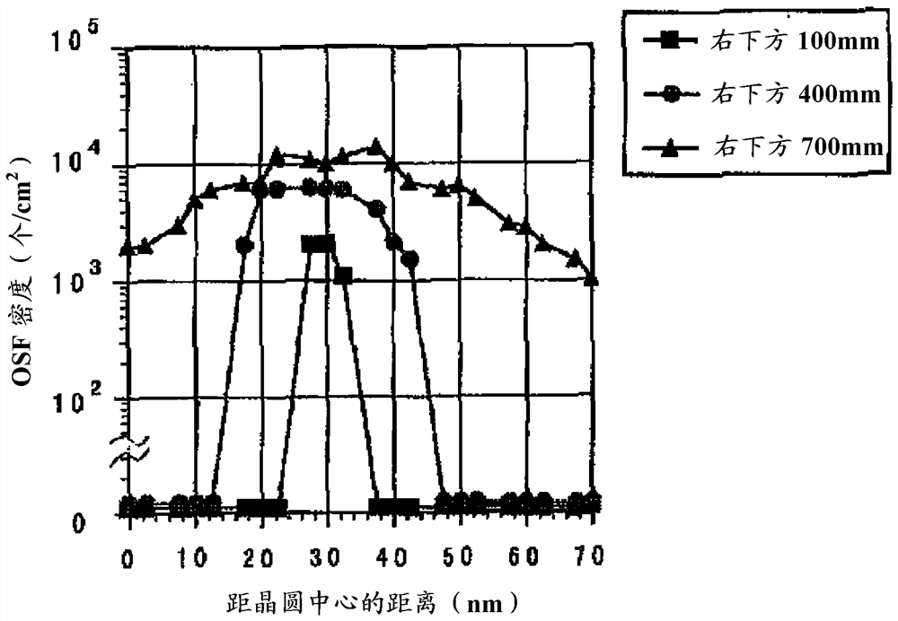
[0066] At 3ppm Cu(NO 3 ) 2 After contaminating the surface of these wafers with a spin coater in an aqueous solution, a model heat treatment assumed in the power device manufacturing process was performed in dry oxygen, and changes in the gettering effect accompanying the heat treatment were investigated.
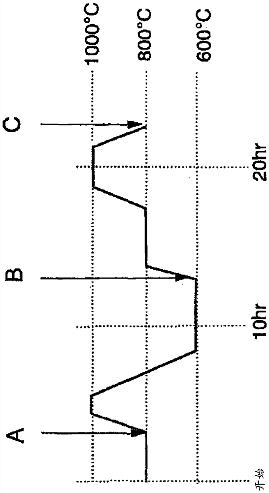
[0067] Figure 4 Indicates the temperature and time conditions of the pattern heat treatment. In the process shown in the figure, the wafer was taken out at three time points shown as A, B, and C, and the effect of gettering accompanying th...
PUM
| Property | Measurement | Unit |
|---|---|---|
| diameter | aaaaa | aaaaa |
| diameter | aaaaa | aaaaa |
| size | aaaaa | aaaaa |
Abstract
Description
Claims
Application Information