Grid-controlled graphene-based ultraviolet-to-near infrared InGaAs detector chip

A detector chip, alkenyl violet technology, applied in semiconductor devices, electrical components, circuits, etc., can solve the problems of large system size and weight, inability to detect ultraviolet light, complex detection system, etc., achieve high photocurrent signal gain and broaden the response Spectrum, the effect of low preparation cost

Inactive Publication Date: 2018-11-27
FUDAN UNIV
View PDF3 Cites 1 Cited by
  • Summary
  • Abstract
  • Description
  • Claims
  • Application Information

AI Technical Summary

Problems solved by technology

The absorption cut-off wavelength of the InGaAs material is in the near-infrared band, which means that the absorption spectrum of the InGaAs material can cover visible light and even ultraviolet light with a wavelength smaller than the near-infrared, but due to the absorption of the InP substrate and the InP cap layer, the InP / InGaAs / InP detectors detect visible light and ultraviolet bands, so that traditional InGaAs detectors cannot detect targets in ultraviolet and visible bands, and cannot identify some widely used lasers with shorter wavelengths.
In addition, for some applications that need to detect ultraviolet light, visible light and short-wave infrared light at the same time, multiple separate detectors are required to detect them separately, which leads to the disadvantages of complex detection system, large system size and weight.

Method used


Image

  • Grid-controlled graphene-based ultraviolet-to-near infrared InGaAs detector chip
  • Grid-controlled graphene-based ultraviolet-to-near infrared InGaAs detector chip

Examples


Embodiment 1

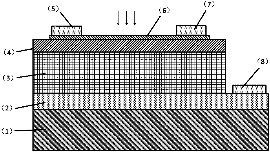
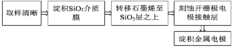
[0025] 1. Sampling and cleaning, using acetone, ethanol and deionized water to ultrasonically clean the sample for 8~3mins;

[0026] 2. Deposit the SiO2 dielectric layer 4 by plasma enhanced chemical vapor deposition (PECVD) technology to deposit the SiO2 dielectric layer 4 with a thickness of 90nm, the substrate temperature is 330±20°C, and the RF power is 40±10W;

[0027] 3. Transfer graphene 6, using dry transfer technology to transfer graphene with a thickness of 1 atomic layer onto the SiO2 dielectric layer 4;

[0028] 4. Etching the contact layer of the open gate electrode, using Ar ion etching technology for etching, the etching conditions are: ion energy 150-400eV, beam current 40-80cm -3 ;

[0029] 5. Deposit metal electrodes, using ion beam sputtering process to deposit metal electrodes, vacuum degree is 2~5×10 -2 Pa, the ion beam energy is 100 eV ~250eV;

[0030] 6. Test results: The response band of the detector covers 375nm~1700nm, and the response rate can rea...

Embodiment 2

[0032] 1. Sampling and cleaning, using acetone, ethanol and deionized water to ultrasonically clean the sample for 8~3mins;

[0033] 2. Deposit SiO2 dielectric layer 4 by plasma enhanced chemical vapor deposition (PECVD) technology to deposit SiO2 dielectric layer 4 with a thickness of 300nm, the substrate temperature is 330±20°C, and the RF power is 40±10W;

[0034] 3. Transfer graphene 6, using dry transfer technology to transfer graphene with a thickness of 3 atomic layers to the SiO2 dielectric layer 4;

[0035] 4. Etching the contact layer of the open gate electrode, using Ar ion etching technology for etching, the etching conditions are: ion energy 150-400eV, beam current 40-80cm -3 ;

[0036] 5. Deposit metal electrodes, using ion beam sputtering process to deposit metal electrodes, vacuum degree is 2~5×10 -2 Pa, the ion beam energy is 100 eV ~250eV;

[0037] 6. Test results: The response band of the detector covers 375nm~1700nm, and the response rate can reach 140A / ...

Embodiment 3

[0039] 1. Sampling and cleaning, using acetone, ethanol and deionized water to ultrasonically clean the sample for 8~3mins;

[0040] 2. Deposit the SiO2 dielectric layer 4 by plasma enhanced chemical vapor deposition (PECVD) technology to deposit the SiO2 dielectric layer 4 with a thickness of 90nm, the substrate temperature is 330±20°C, and the RF power is 40±10W;

[0041] 3. Transfer graphene 6, using dry transfer technology to transfer graphene with a thickness of 5 atomic layers to the SiO2 dielectric layer 4;

[0042] 4. Etching the contact layer of the open gate electrode, using Ar ion etching technology for etching, the etching conditions are: ion energy 150-400eV, beam current 40-80cm -3 ;

[0043] 5. Deposit metal electrodes, using ion beam sputtering process to deposit metal electrodes, vacuum degree is 2~5×10 -2 Pa, the ion beam energy is 100 eV ~250eV;

[0044] 6. Test results: The response band of the detector covers 375nm~1700nm, and the response rate can reac...


PUM

PropertyMeasurementUnit
Thicknessaaaaaaaaaa

Abstract

The invention belongs to the technical field of detector chips and particularly relates to a grid-controlled graphene-based ultraviolet-to-near infrared InGaAs detector chip. According to the invention, a InP contact layer, a InGaAs absorption layer, a silicon oxide (SiO2) medium layer, a graphene layer, a source electrode metal electrode, a drain electrode metal electrode and a grid electrode metal electrode are successively arranged on a InP substrate. The chip is advantageous in that on one hand, by using a grid-controlled interface field to separate photon-generated carriers, and sensing inversion type carriers in the graphene, spectrum detection is achieved; on the other hand, the graphene is free from energy gap and quite high in optical permeability; the InGaAs materials are capableof absorbing light of the 1.7[mu]m to ultraviolet wave band, so by use of the detector, detection from the ultraviolet to near infrared waveband can be achieved; and in addition, the graphene has quite high migration rate and carrier transmission characteristics, so the detector is enabled to have quite high quantum gain characteristics.

Description

technical field [0001] The invention belongs to the technical field of detector chips, in particular to a grid-controlled graphene-based ultraviolet to near-infrared InGaAs detector chip. Background technique [0002] The traditional structure of indium gallium arsenide detector chip is indium phosphide (InP) / indium gallium arsenide (InGaAs) / indium phosphide InP structure, which has good performance in the near infrared band, which makes it widely used in civil, military and aviation Aerospace field has a wide range of application value. The absorption cut-off wavelength of the InGaAs material is in the near-infrared band, which means that the absorption spectrum of the InGaAs material can cover visible light and even ultraviolet light with a wavelength smaller than the near-infrared, but due to the absorption of the InP substrate and the InP cap layer, the InP / InGaAs / InP detectors detect visible light and ultraviolet bands, so that traditional InGaAs detectors cannot dete...

Claims


Application Information

Patent Timeline
IPC IPC(8): H01L31/028H01L31/112H01L31/0216
CPCH01L31/02167H01L31/028H01L31/112
Inventor 曹高奇仇志军丛春晓邵秀梅李雪胡来归龚海梅
Owner FUDAN UNIV
Why Eureka
Try Eureka