ZnMgO ultraviolet detector
A technology of ultraviolet detectors and thin-film layers, applied in semiconductor devices, electrical components, circuits, etc., can solve problems affecting the crystal quality of thin films and the comprehensive performance of devices, and achieve easy control of the reaction process, simple preparation process, and good light effects effect of ability
- Summary
- Abstract
- Description
- Claims
- Application Information
AI Technical Summary
Problems solved by technology
Method used
Image
Examples
Embodiment 1
[0057] 1.1 Use trichloroethylene, acetone, and ethanol to clean the sapphire substrate, and then dry it with dry nitrogen. (The thickness of the substrate is 0.45~0.55mm, the scale is 2 inches, and the square is about 5-10mm×5-10mm after cutting)
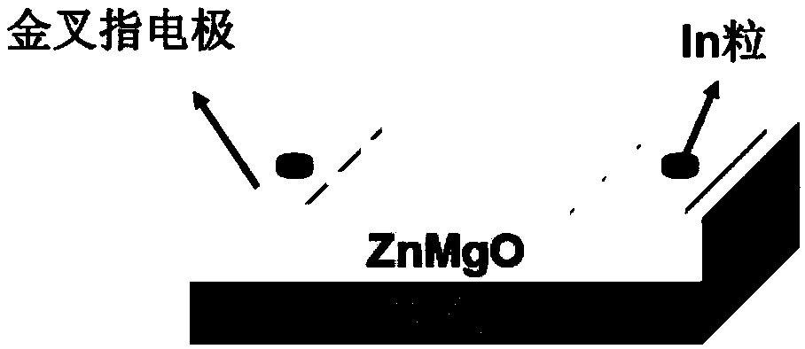
[0058] 1.2 Put the sapphire substrate in 1.1 into the MOCVD growth equipment, adjust the growth temperature to 450°C, and the vacuum degree of the growth chamber to 1×10 4 Pa, use diethylzinc as the zinc source, dimethylmagnesocene as the magnesium source, the molar concentration ratio of zinc and magnesium is adjusted with different high-purity nitrogen carrier gas ratios, the flow rate of oxygen is 150mL / min, diethyl The carrier gas flow rate of the base zinc pipeline is 15mL / min, and the carrier gas flow rate of the dimethylmagnesocene pipeline is 50mL / min.
[0059] 1.3 Grow for 2 hours, turn off the organic source, reduce the temperature at a cooling rate of 5°C / min, and finally reduce to room temperature, take out the substrate, and...
Embodiment 2
[0065] In order to examine the influence of the oxygen flow rate on the preparation of the device, only the oxygen flow rate was changed, and the other conditions were the same as in Example 1, and a series of ultraviolet light detection devices were obtained. The oxygen flow rates are 750 mL / min, 1350 mL / min, and 1850 mL / min.
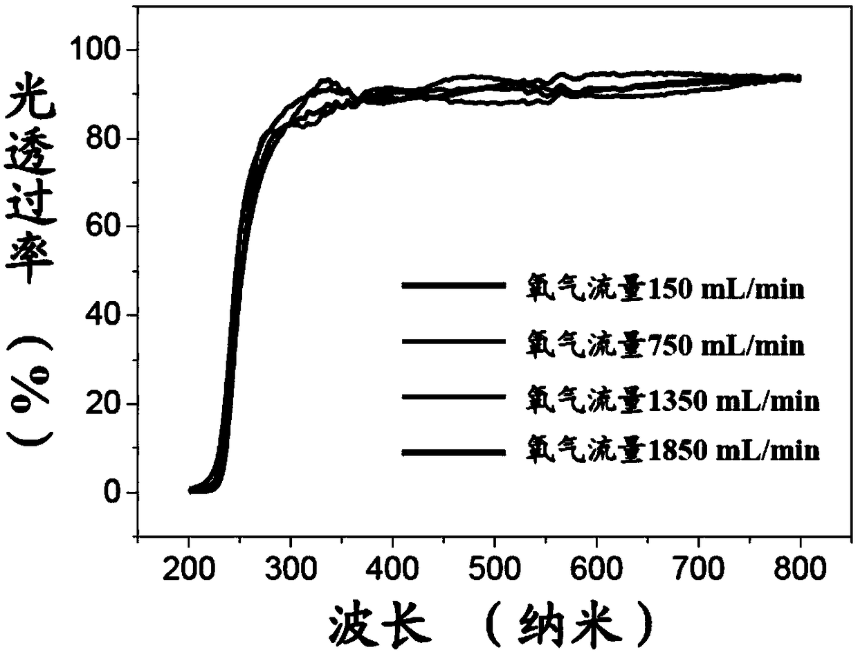
[0066] figure 2 It is the ultraviolet-visible light absorption spectrum of the ZnMgO film layer. It can be seen from the figure that with the change of the oxygen flow rate, the light absorption cut-off edge of the ZnMgO film layer does not change, and they are all located near 230nm.
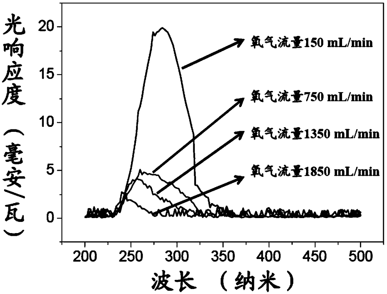
[0067] The light response of the ZnMgO ultraviolet detector obtained in Example 2 was detected, and the light response spectrum was obtained as image 3 As shown, it can be seen from the figure that the light response cut-off edge of the devices prepared under different oxygen flow conditions has changed significantly, from 350nm to around 275nm.
Embodiment 3
[0069] 3.1 Use trichloroethylene, acetone, and ethanol to clean the sapphire substrate, and then dry it with dry nitrogen. (The thickness of the substrate is 0.45~0.55mm, the scale is 2 inches, and the square is about 5-10mm×5-10mm after cutting)
[0070] 3.2 Put the sapphire substrate in 3.1 into the MOCVD growth equipment, adjust the growth temperature to 450°C, and the vacuum degree of the growth chamber to 1×10 4 Pa, use diethylzinc as the zinc source, dimethylmagnesocene as the magnesium source, the molar concentration ratio of zinc and magnesium is adjusted with different high-purity nitrogen carrier gas ratios, the flow rate of oxygen is 150mL / min, diethyl The carrier gas flow rate of the base zinc pipeline is 15mL / min, and the carrier gas flow rate of the dimethylmagnesocene pipeline is 80mL / min.
[0071] 3.3 Grow for 2 hours, turn off the organic source, reduce the temperature at a cooling rate of 5°C / min, and finally reduce to room temperature, take out the substrate, and...
PUM
 Abstract
Description
Claims
Application Information


