
A method for improving field emission performance of carbon nanotube arrays

A carbon nanotube array and nanotube array technology, applied in the field of preparation and application of nanomaterials, can solve the problems of low field emission current density, large number of field emission points, poor stability, etc., and achieve work function reduction, field emission Effects of Enhanced Electron Emission Capability and Enhanced Tube-Base Bonding

Inactive Publication Date: 2018-12-11
TIANJIN NORMAL UNIVERSITY
View PDF4 Cites 4 Cited by
  • Summary
  • Abstract
  • Description
  • Claims
  • Application Information

AI Technical Summary

Problems solved by technology

[0003] The purpose of the present invention is to overcome the disadvantages of the existing carbon nanotube-based field emission cathode that the working electric field is relatively high, the field emission current density is small, and the stability is not good during high current density field electron emission. Microwave nitrogen and hydrogen plasma treatment, obtained nitrogen-doped silicon carbide-carbon nanotube array composite material with low work function and large number of field emission points, and finally obtained a combination of ultra-low working electric field, ultra-large field emission current density and Carbon nanotube-based field emission cathode material with good field emission stability at high current density

Method used


Image

  • A method for improving field emission performance of carbon nanotube arrays
  • A method for improving field emission performance of carbon nanotube arrays
  • A method for improving field emission performance of carbon nanotube arrays

Examples


Embodiment 1

[0028] (1) Pretreatment of silicon single wafer:

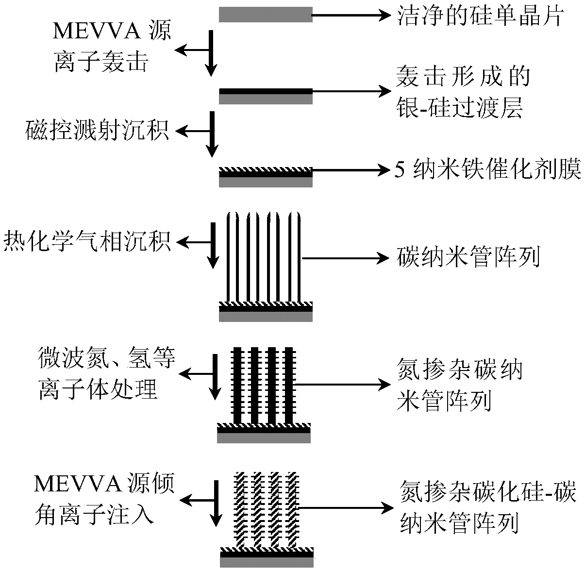
[0029] First, the n-type (100) silicon single wafer cut into small pieces of 2cm×2cm was cleaned ultrasonically (50W) in deionized water and absolute ethanol for 5 minutes, and then immersed in hydrofluoric acid with a volume ratio of 4%. After 5 minutes, take it out and dry it in the air, and then carry out energy-carrying silver ion bombardment pretreatment in the silicon single wafer with the clean surface obtained in the metal vapor vacuum arc ion source (MEVVA source). During the bombardment, keep the sample stage rotating at a constant speed. The bias voltage is set to -15kV, the beam current is 10 mA, and the bombardment time is 10 minutes. The bombardment pretreatment process can be used to improve the binding force between the carbon nanotubes and the substrate.

[0030] (2) Preparation of carbon nanotube arrays by thermal chemical vapor deposition and annealing at high temperature:

[0031] Put the silicon single wa...

Embodiment 2

[0037] (1) Pretreatment of silicon single wafer:

[0038] First, the n-type (100) silicon single wafer cut into small pieces of 2cm×2cm was cleaned ultrasonically (50W) in deionized water and absolute ethanol for 5 minutes, and then immersed in hydrofluoric acid with a volume ratio of 4%. After 5 minutes, take it out and dry it in the air, and then carry out energy-carrying silver ion bombardment pretreatment in the silicon single wafer with the clean surface obtained in the metal vapor vacuum arc ion source (MEVVA source). During the bombardment, keep the sample stage rotating at a constant speed. The bias voltage was set to -15 kV, the beam current was 10 mA, and the bombardment time was 10 minutes.

[0039] (2) Preparation of carbon nanotube arrays by chemical vapor deposition:

[0040] Put the silicon single wafer obtained in step (1) into a magnetron sputtering device to deposit a thickness of 5 nanometers of iron catalyst film, then put it into a high temperature quartz...

Embodiment 3

[0046] (1) Pretreatment of silicon single wafer:

[0047] First, the n-type (100) silicon single wafer cut into small pieces of 2cm×2cm was cleaned ultrasonically (50W) in deionized water and absolute ethanol for 5 minutes, and then immersed in hydrofluoric acid with a volume ratio of 4%. After 5 minutes, take it out and dry it in the air, and then carry out energy-carrying silver ion bombardment pretreatment in the silicon single wafer with the clean surface obtained in the metal vapor vacuum arc ion source (MEVVA source). During the bombardment, keep the sample stage rotating at a constant speed. The bias voltage was set to -15 kV, the beam current was 10 mA, and the bombardment time was 10 minutes.

[0048] (2) Preparation of carbon nanotube arrays by chemical vapor deposition:

[0049] Put the silicon single wafer obtained in step (1) into a magnetron sputtering device to deposit a thickness of 5 nanometers of iron catalyst film, then put it into a high temperature quartz...


PUM

PropertyMeasurementUnit
Maximum field emission current densityaaaaaaaaaa

Abstract

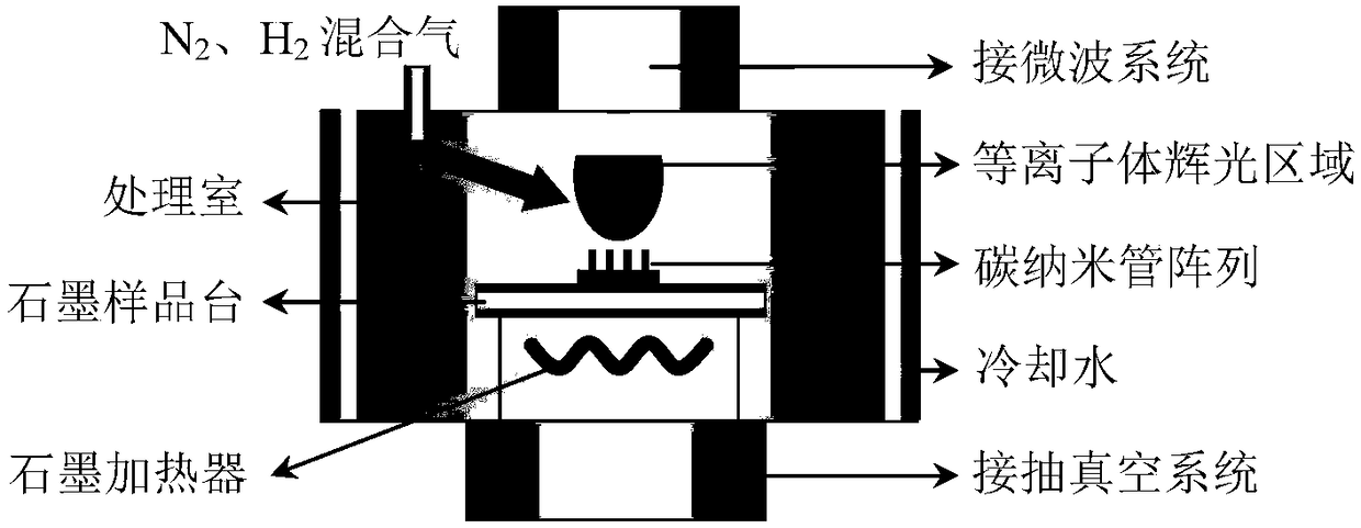
The invention discloses a method for improving field emission performance of a carbon nanotube array, belonging to the field of preparation and application of nano materials. Includes such steps 1, ascarrying out energetic silver ion bombardment pretreatment on monocrystalline silicon wafer; (2) preparing carbon nanotube arrays by conventional thermochemical vapor deposition and annealed at hightemperature; 3) treating the carbon nanotube arrays at room temperature with nitrogen and hydrogen plasma in a microwave plasma system; (4) Carrying out energetic silicon ion bombardment on carbon nanotubes by means of inclined angle implantation. Compared with pure carbon nanotube arrays and prior art, the nitrogen-doped silicon carbide prepared by the method has the advantages that: the Carbon nanotube arrays have very low working electric field and very high field emission current density, and excellent field emission stability at high field emission current density, so they have very highapplication value.

Description

technical field [0001] The invention belongs to the technical field of preparation and application of nanomaterials, and in particular relates to a method for preparing nitrogen-doped silicon carbide-carbon nanotube arrays by plasma treatment and improving their field electron emission performance. Background technique [0002] As a quasi-one-dimensional nanomaterial, carbon nanotubes have good electrical conductivity, mechanical strength and high chemical inertness. They have shown good application prospects in many fields such as energy storage, transistors, material composite enhancements, and detectors. . At the same time, the extremely large aspect ratio of carbon nanotubes also makes it an ideal field emission cathode material, showing good application potential in the development of vacuum field electronic devices. Field emission refers to the process of electrons inside the cathode material escaping from the surface of the material into the vacuum under the action o...

Claims


Application Information

Patent Timeline
IPC IPC(8): H01J1/304H01J9/02B82Y30/00B82Y40/00
CPCB82Y30/00B82Y40/00H01J1/304H01J9/025H01J2201/30434H01J2201/30469H01J2201/30484H01J2209/0223
Inventor 邓建华张燕朱文祥
Owner TIANJIN NORMAL UNIVERSITY
Learn More