A method for reducing the ohmic contact resistance of a wide band gap semiconductor device

A wide bandgap semiconductor and ohmic contact electrode technology, which is applied in the field of reducing the ohmic contact resistance of III-V wide bandgap semiconductor devices, can solve problems greater than 0.5Ω, etc., to reduce ohmic contact resistance, increase ohmic contact area, enhance The effect of device performance

Pending Publication Date: 2019-01-15
NAT UNIV OF SINGAPORE +2
View PDF5 Cites 12 Cited by
  • Summary
  • Abstract
  • Description
  • Claims
  • Application Information

AI Technical Summary

Problems solved by technology

The main disadvantage of this type of ohmic contact manufacturing method is that the contact area between the multilayer metal and the wide bandgap semiconductor material is the same as or smaller than the area of ​​the ohmic contact area, and the optimization of the resistivity of the ohmic contact is mainly by adjusting the thickness combination of the multilayer metal. achieved with annealing conditions, but this method yields ohmic contact resistances typically greater than 0.5Ω·mm

Method used


Image

  • A method for reducing the ohmic contact resistance of a wide band gap semiconductor device
  • A method for reducing the ohmic contact resistance of a wide band gap semiconductor device
  • A method for reducing the ohmic contact resistance of a wide band gap semiconductor device

Examples


Embodiment 1

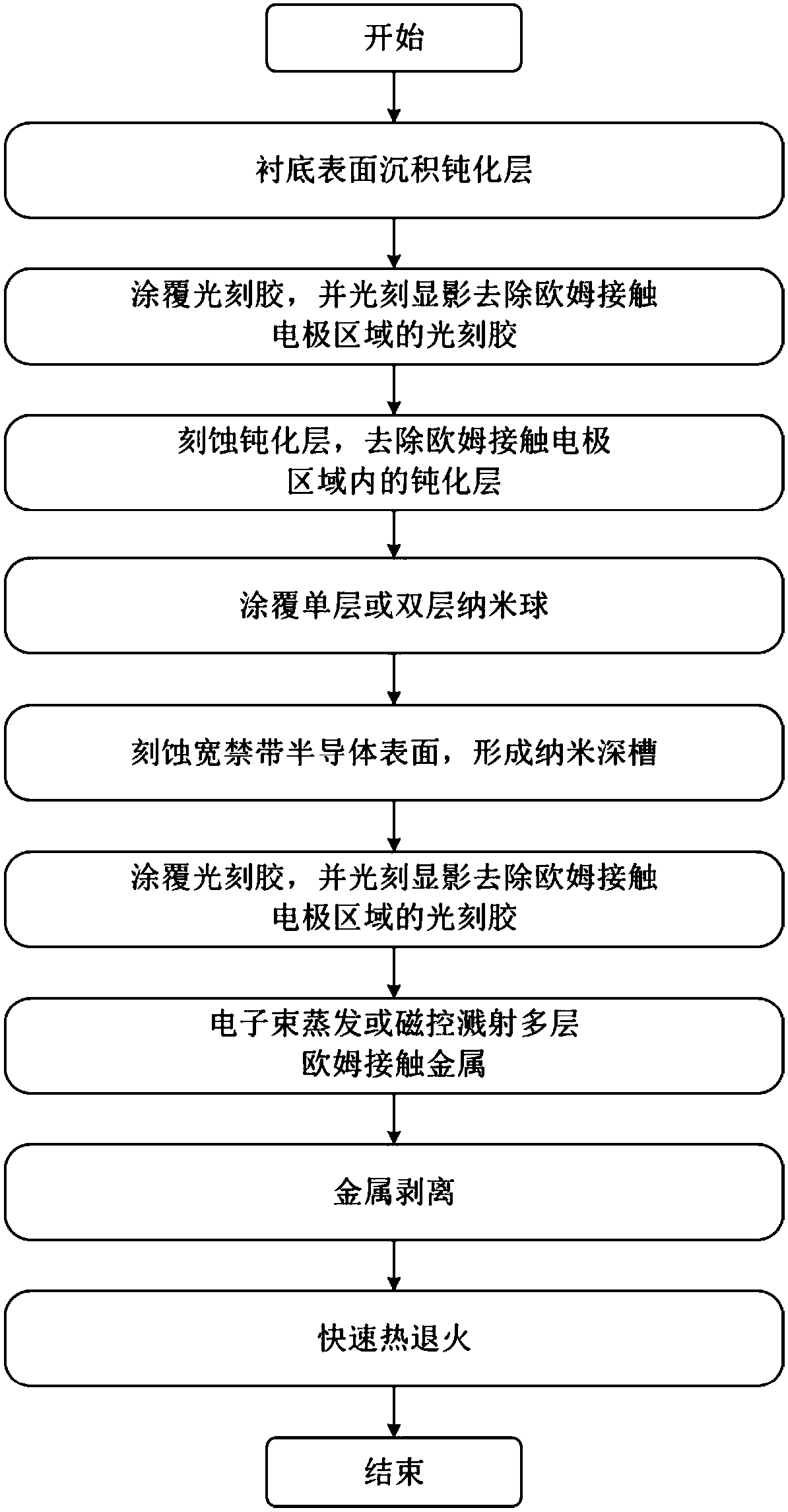
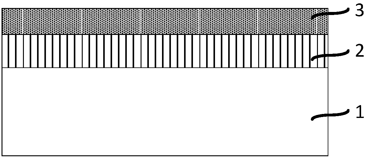
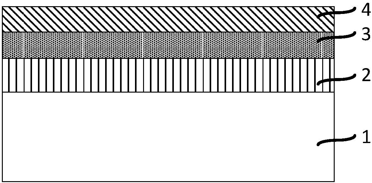
[0057] Step 1, depositing a passivation layer, the material is Si 3 N 4

[0058] Deposit a layer of 100nm Si on the surface of wide band gap semiconductor material by PECVD (plasma enhanced chemical vapor deposition) 3 N 4 passivation layer;

[0059] Step 2, apply photoresist, and photolithographic development to remove the photoresist in the ohmic contact electrode area

[0060] Coat photoresist AZ5214E ​​on the passivation layer deposited in step 1, pre-bake at 90°C for 90s, expose to ultraviolet light for 6s, develop with 2.38% tetramethylammonium hydroxide solution for 45s, and remove the photoresist in the ohmic contact electrode area glue to form a photoresist window, and post-bake at 110°C for 30s;

[0061] Step 3, etch the passivation layer, remove the passivation layer in the ohmic contact electrode area, and remove the photoresist

[0062] The passivation layer is etched by RIE (Reactive Ion Etching), and the working gas is CF 4 with O 2 , RF power 100W, time...

Embodiment 2

[0076] Step 1, depositing a passivation layer, the material is SiO 2

[0077] Using ICPCVD (inductively coupled plasma chemical vapor deposition) to deposit a layer of 50nm SiO on the surface of wide bandgap semiconductor materials 2 passivation layer;

[0078] Step 2, apply photoresist, and photolithographic development to remove the photoresist in the ohmic contact electrode area

[0079] Coat photoresist AZ5214E ​​on the passivation layer deposited in step 1, pre-bake at 90°C for 90s, expose to ultraviolet light for 6s, develop with 2.38% tetramethylammonium hydroxide solution for 45s, and remove the photoresist in the ohmic contact electrode area glue to form a photoresist window, and post-bake at 110°C for 30s;

[0080] Step 3, etch the passivation layer, remove the passivation layer in the ohmic contact electrode area, and remove the photoresist

[0081] ICPRIE (Inductively Coupled Plasma Etching) is used to etch the passivation layer, and the working gas is SF 6 wi...


PUM

PropertyMeasurementUnit
thicknessaaaaaaaaaa
diameteraaaaaaaaaa
thicknessaaaaaaaaaa

Abstract

The invention discloses a method for reducing the ohmic contact resistance of a wide band gap semiconductor device, wherein the material of the wide band gap semiconductor device is III- V-group wide-band gap semiconductor material that comprises a substrate, a buffer lay, a channel layer and an alloy barrier layer sequentially arranged from bottom to top. That method comprise the following steps:depositing a passivation layer; 2, coating photoresist and forming a photoresist window; 3, etching that passivation layer and for a window of the passivation layer; 4, coating a nano ball; 5, forming a nano groove; 6, coating photoresist and forming a photoresist window; 7, evaporating the electron beam or magnetron sputtering the multi-layer metal; Step 8, peeling off the multi-layer metal; Step 9: Rapidly carrying out thermal annealing to form ohmic contact. The method of the invention greatly increases the contact area between the electrode metal and the wide band gap semiconductor, reduces the ohmic contact resistance of the wide band gap semiconductor device, enhances the device performance, improves the process efficiency, and reduces the process cost.

Description

technical field [0001] The invention relates to the technical field of wide bandgap semiconductors, in particular to a method for reducing the ohmic contact resistance of III-V wide bandgap semiconductor devices based on nanosphere photolithography and plasma etching technology. Background technique [0002] III-V wide bandgap semiconductor devices have the advantages of wide direct bandgap, high electron saturation drift velocity, high breakdown field strength, corrosion resistance and radiation resistance. Compared with silicon-based devices, wide-bandgap semiconductor devices have high switching speed, low on-resistance, greatly improved power density, and can work in high-temperature environments. The quality of the ohmic contact of the wide bandgap semiconductor device determines the working performance of the device to a large extent. The current common method to achieve ohmic contacts for wide bandgap power devices involves conducting multilayer metals (usually Ti / Al...

Claims


Application Information

Patent Timeline
Patent Type & Authority Applications(China)
IPC IPC(8): H01L21/28H01L29/45B82Y40/00
CPCH01L29/401H01L29/452B82Y40/00
Inventor 孙瑞泽梁永齐赵策洲蔡宇韬
Owner NAT UNIV OF SINGAPORE
Why Eureka
Try Eureka