Method for chemical plating on surface of polymer film

A technology of polymer film and surface chemistry, which is applied in the field of electroless plating, can solve problems such as environmental pollution and surface damage, and achieve the effect of reducing cost and good activation effect

Active Publication Date: 2019-04-05
SHANGHAI JIAO TONG UNIV
View PDF5 Cites 2 Cited by
  • Summary
  • Abstract
  • Description
  • Claims
  • Application Information

AI Technical Summary

Problems solved by technology

However, hexavalent chromium ions are usually used for surface roughening, which seriously pollutes the environment, and surface plasma treatment will cause certain damage to the surface

Method used


Image

  • Method for chemical plating on surface of polymer film
  • Method for chemical plating on surface of polymer film
  • Method for chemical plating on surface of polymer film

Examples


Embodiment 1

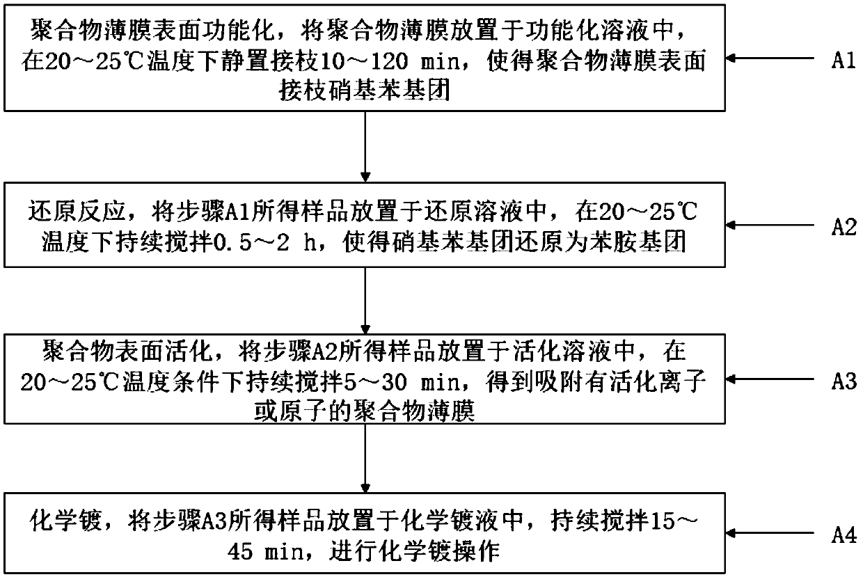
[0039] refer to figure 1 , present embodiment provides a kind of method of electroless plating on polymer film surface, polymer film can be polymethyl methacrylate (PMMA), polymethacrylic acid (PMAA), polymethacrylimide (PMI) , polyethylene terephthalate (PET), polyamide (PA), polypropylene (PP), polyvinyl chloride (PVC), polyvinyl alcohol (PVA) and most organic films, and the thickness of the polymer film It can be as low as several hundred nanometers, can be deposited on a metal or semiconductor substrate, and the polymer film can be prepared by conventional methods in the art. The method of this embodiment includes:

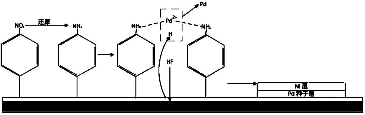
[0040] A1: The surface of the polymer film is functionalized, the polymer film is placed in a functional solution, and the grafting is allowed to stand at a temperature of 20-25°C for 10-120 minutes, so that the surface of the polymer film is grafted with nitrophenyl groups;

[0041] A2: Reduction reaction, place the sample obtained in step A1 in the reducin...

Embodiment 2

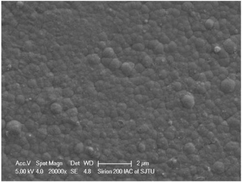
[0060] The substrate is a silicon wafer, and the surface of a polymethyl methacrylate (PMMA) film with a thickness of 200nm is chemically plated with Ni-P alloy. The specific steps are:

[0061] 1. Preparation of PMMA film: use acetone, alcohol and deionized water respectively for a size of 1×2cm 2 After the silicon chip was ultrasonically cleaned, it was immersed in an HF solution with a volume ratio concentration of 5% for Si–H treatment for 3 minutes, and the silicon chip was placed in the prepared grafting solution, and the grafting reaction was carried out at room temperature for 45 minutes. Afterwards, they were ultrasonically cleaned with deionized water and dried. A PMMA polymer film with a thickness of about 200 nm was obtained on the surface of the silicon wafer. The preparation method of the above-mentioned grafting solution is as follows: first, add 50 mL of deionized water into a beaker, then add 0.1 g of sodium lauryl sulfate, 1 mL of fluoroboric acid, 0.5 mL of...

Embodiment 3

[0073] Substrate is copper, and thickness is the polymethacrylic acid (PMAA) film surface electroless Ni-P alloy plating of 1 μm, and its step is:

[0074] 1. Preparation of PMAA film: the size is 1×2cm 2 The copper sheet was placed in the chemical grafting solution of PMAA, and after the grafting reaction was carried out at room temperature for 30 minutes, it was ultrasonically cleaned with deionized water and dried. A PMAA polymer film with a thickness of about 150 nm was obtained on the surface of the copper sheet. The preparation method of the grafting solution is as follows: first, add 50 mL of deionized water into the beaker, then add 0.1 g of sodium lauryl sulfate, 1 mL of fluoroboric acid, 0.5 mL of hydrofluoric acid, and 2 mL of formazan in sequence under magnetic stirring. Acrylic acid and 0.1 g of diazonium p-nitrobenzenetetrafluoroborate were stirred until a clear solution was obtained.

[0075] 2. Set the size to 1×2cm 2 The samples were ultrasonically cleaned ...


PUM

PropertyMeasurementUnit
Thicknessaaaaaaaaaa
Thicknessaaaaaaaaaa

Abstract

The invention discloses a method for chemical plating on a surface of a polymer film. The method for chemical plating on the surface of the polymer film comprises the following steps that the surfaceof the polymer film is functionalized at first, so that the surface of the polymer film is grafted with nitrobenzene groups; then the nitrobenzene groups are reduced into aniline groups; the polymer film which is reduced to the aniline groups is placed in an activation solution containing hydrofluoric acids for activation, so that the surface with the catalytic activity is obtained; and finally, the chemical plating operation is carried out. According to the method for chemical plating on the surface of the polymer film, the nitrobenzene groups are grafted on the surface of a polymer and thenare reduced into the anilines, the aniline groups have a relatively strong adsorption effect on activated ions or atoms, so that the polymer film is activated to obtain the surface with the catalyticactivity and the surface of the polymer film is smoothly plated with a metal layer. According to the method for chemical plating on the surface of the polymer film, the surface functionalization stepis designed, the problems that the surface energy of the polymer is low and cannot become a catalytic surface are solved, and negative effects caused by surface coarsening and surface plasma treatmentare avoided.

Description

technical field [0001] The invention belongs to the technical field of electroless plating, in particular to a method for electroless plating on the surface of a polymer film Background technique [0002] Due to the good thermal stability, insulation and optoelectronic properties of polymer films, they have been increasingly used in microelectronic packaging, automotive industry and optoelectronic devices in recent years. The metallization of polymer films has thus attracted extensive attention. However, metallization of polymer films is a challenge due to their low surface energy and inherently weak adhesion. Commonly used metallization methods for polymer films include magnetron sputtering, physical vapor deposition, and chemical vapor deposition. However, these methods have high environmental requirements and often need to be carried out under vacuum conditions, and the equipment is expensive and the operation is complicated, which limits their application. Electroless...

Claims


Application Information

Patent Timeline
IPC IPC(8): C23C18/20C23C18/30C23C18/36C23C18/50C23C18/52
CPCC23C18/2086C23C18/30C23C18/36C23C18/50C23C18/52
Inventor 熊立双刘阳杭弢吴蕴雯高立明李明
Owner SHANGHAI JIAO TONG UNIV
Why Eureka
Try Eureka