
Preparation method of pcb board with prefabricated solder and pcb board

A PCB board and solder technology, which is applied in the field of PCB board preparation, can solve the problems of increasing the technical difficulty of micropowder preparation, the increase of preparation cost, and the complexity of the process, so as to achieve easy personalized circuit design and agile manufacturing, eliminate waste liquid pollution discharge, The effect of broad application prospects

Active Publication Date: 2020-09-01
BEIJING COMPO ADVANCED TECH
View PDF6 Cites 0 Cited by
  • Summary
  • Abstract
  • Description
  • Claims
  • Application Information

AI Technical Summary

Problems solved by technology

Moreover, with the development of packaging on board (COB), flip chip technology (FC), and stacked (POP) packaging technology, more and more ultra-fine solder paste is printed, and the printing stencil is getting thinner and thinner. It will cause printing offset, and the stencil with tiny mesh also greatly increases the missing printing rate of solder paste; It increases the technical difficulty of micropowder preparation, and it will cause the refinement of the powder to increase the specific surface area, which will cause the total oxygen content to exceed the standard, resulting in tin beads and poor wetting.
This greatly increases the preparation cost, and this problem will become more and more serious with the development of electronic information products
[0004] In the face of the wide application of new ultra-small components, the use of solder paste to print solder paste on the pad by traditional screen or stencil printing has reached the limit of the equipment, while the existing solder paste printing process, Not only the process is complicated, but also the clogging of the nozzle is easy to cause inconsistent pads, causing defects such as device tombstoning and false soldering

Method used


Image

  • Preparation method of pcb board with prefabricated solder and pcb board

Examples


Embodiment 1

[0023] The preparation method of embodiment 1 single-layer PCB board 1

[0024] First, use FR-4 epoxy resin as the base material to make the PCB core board, bake the core board at 150°C for 4 hours, remove the water vapor in the board, further cure the resin, and eliminate the internal stress of the board. Cut the substrate according to the cutting size of 580mm×470mm, take the middle part of 550mm×440mm as the final product size, and leave a process edge around the substrate to facilitate lamination and alignment in the subsequent production process. Grinding and rounding the substrate to keep the edges and corners of the substrate flat and round, and then use a plate washer to remove resin, dust, impurities, etc. exposed on the surface of the substrate, roughen the surface, and increase adhesion for subsequent processing .

[0025] Secondly, according to the predetermined PCB circuit diagram, through the thermal spraying process, use the numerical control equipment to unifo...

Embodiment 2

[0029] The preparation method of embodiment 2 multilayer PCB board 2

[0030] The same process as in Example 1 is used to prepare six PCB boards with different solder circuit patterns, wherein in this method, the tin solder powder adopts 25-45 μm SnZn9 alloy powder, and after electrostatic spraying, it is necessary to use a miniature impact hammer to solder the solder circuit. Ultrasonic hammering for densification.

[0031] Lay six PCB boards with conductive circuit patterns in sequence according to the design requirements, and through the pre-made target holes, the patterns between the layers can be accurately aligned to avoid misalignment and open circuits that affect the reliability of the product. The PCB boards are bonded and laminated through the prepreg to obtain a six-layer PCB. Finally, use a numerical control spray gun to evenly spray a layer of adjusted flux on the reserved tin solder pad, and seal it up after the flux solidifies. After testing, under the prepara...

Embodiment 3

[0033] The preparation method of the FPC board 3 (flexible circuit board) of embodiment 3 double-sided preset solder

[0034] First, polyimide is used as the base material to manufacture FPC flexible core boards, and the soft boards are pretreated by cutting, cleaning, surface roughening, etc., to remove dust and impurities exposed on the substrate surface, and to increase adhesion for subsequent processing . On the upper and lower surfaces of the processed board core, use the same process steps as in the embodiment to form solder lines, welding bosses and insulating solder resist layers in turn, and then use the same process steps as in Example 1 to weld the bosses. The surface is sprayed with flux, and it can be sealed after the flux solidifies. After testing, under the preparation method, the yield can reach 99%.

[0035]The front and back sides of the FPC board 3 prepared by this method are all provided with single-layer solder lines and solder bosses, the solder bosses ...


PUM

PropertyMeasurementUnit
particle sizeaaaaaaaaaa
thicknessaaaaaaaaaa

Abstract

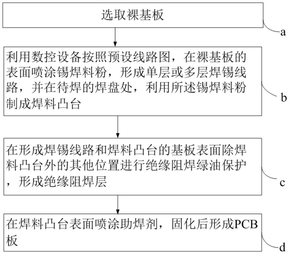
The invention relates to a preparation method of a PCB with pre-prepared solder and the PCB. The preparation method of the PCB comprises the following steps: (a) selecting a bare substrate; (b) spraying tin solder powder on the surface of the bare substrate by utilizing a numerical control device according to a preset circuit diagram to form single-layer or multi-layer tin soldering circuits, andmanufacturing a solder boss by utilizing the tin solder powder at the position corresponding to a solder pad to serve as the solder pad; (c) carrying out insulative solder-resistant green oil protection on the residual portion except the position of the solder boss on the surface on which the solder circuits and the solder boss are formed to form an insulative solder-resistant layer; (d) sprayinga soldering flux on the surface of the solder boss, and executing curing to form the PCB. The PCB is prepared by the preparation method. The compatibility problem between the heterogeneous interfacesof the solder pad and the circuits in the assembly process of the PCB with traditional copper circuits is solved, tin soldering paste and a printing process are omitted, and the problems of offset printing, missed printing and the like in the printing process of the solder paste with narrow spacing and fine granularity can be eliminated, so that the yield is greatly improved.

Description

technical field [0001] The invention relates to the technical field of PCB board preparation, in particular to a preparation method of a PCB board with prefabricated solder and the PCB board. Background technique [0002] Printed circuit board (referred to as PCB board: Printed Circuit Board), as a support for electronic components, is an important electronic component. The current conventional PCB board processing process includes: copper clad laminate - blanking - chemical cleaning - film - graphics transfer - chemical development - etching and other seven processes. Specifically, the surface of the substrate is covered with copper, a dry film is pasted on the copper-clad board, the pattern is transferred through exposure, and then the PCB board with copper lines can be obtained through chemical development and chemical etching. The above-mentioned production process has many and complicated procedures, long production cycle, high cost, and high energy consumption. In add...

Claims


Application Information

Patent Timeline
Patent Type & Authority Patents(China)
IPC IPC(8): H05K3/28H05K3/34H05K3/40H05K1/11
CPCH05K1/116H05K3/282H05K3/3489H05K3/4007
Inventor 胡强王志刚张富文安宁林刚张江松张品卢彩涛徐蕾赵朝辉赵新明贺会军张焕鹍
Owner BEIJING COMPO ADVANCED TECH
Learn More