

Composite thin film solar cell and preparation method thereof
A technology of solar cells and composite thin films, applied in circuits, electrical components, photovoltaic power generation, etc., can solve the problem of low battery conversion efficiency, copper indium gallium selenide thin film batteries due to scarcity of raw materials, unsuitable for large-scale application of copper zinc tin sulfur thin films and other problems, to achieve the effect of improving photoelectric conversion efficiency, solving low conversion efficiency and improving firmness
- Summary
- Abstract
- Description
- Claims
- Application Information
AI Technical Summary
Problems solved by technology
Method used
Image


Examples
preparation example Construction
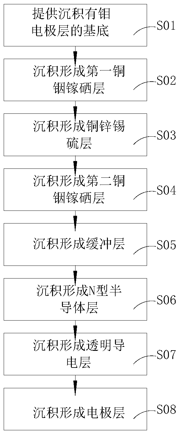
[0048] see figure 2 , the preparation method of the composite thin film solar cell comprises the following steps:
[0049] S01. Provide a substrate deposited with a molybdenum electrode layer; that is, a layer of molybdenum electrode layer is stacked on the surface of the substrate. For example, molybdenum can be coated on the substrate by electron beam coating process, sputtering process, chemical vapor deposition (CVD) process or metal organic chemical vapor deposition (MOCVD) process.
[0050] S02. Depositing a first copper indium gallium selenide layer on the surface of the molybdenum electrode layer by using a pulsed laser deposition method.
[0051] Specifically, in step S02, the diameter of the target is 50mm, the thickness is 3-8mm, the temperature of the substrate is controlled at 400-450°C, the distance from the target to the substrate is 35-45mm, and the laser wavelength of the pulsed laser is 240-250nm , the frequency is 8-16 Hz, the pulse energy is 250-400 mill...
Embodiment 1
[0063] Embodiment 1 provides a composite thin film solar cell and a preparation method thereof. Wherein, the composite thin film solar cell has such figure 1 The structure shown, that is, includes:
[0064] Substrate 1, the substrate 1 is K9 glass;
[0065] molybdenum electrode layer 2, the molybdenum electrode layer 2 is stacked on the surface of the substrate 1;
[0066] A light-absorbing composite layer 3, the light-absorbing composite layer 3 includes a first copper indium gallium selenide layer 31 stacked on the surface of the molybdenum electrode 2, a copper zinc tin sulfur layer stacked on the surface of the first copper indium gallium selenide layer 31 32 and the second copper indium gallium selenide layer 33 stacked on the surface of the copper zinc tin sulfur layer 32, wherein the thickness of the first copper indium gallium selenide layer 31 is 100 nm, the thickness of the copper zinc tin sulfur layer 32 is 800 nm, and the thickness of the first copper indium gall...
PUM
| Property | Measurement | Unit |
|---|---|---|
| thickness | aaaaa | aaaaa |
| thickness | aaaaa | aaaaa |
| thickness | aaaaa | aaaaa |
Abstract
Description
Claims
Application Information