Indium-arsenic-nitrogen-bismuth semiconductor material, laser using material, detector and preparation method

A technology of indium arsenic bismuth nitrogen and semiconductors, which is applied in the field of semiconductor photoelectric material preparation, can solve the problem of low solubility of N atoms, and achieve the effects of easy control, easy growth, simple structure and operation process

Active Publication Date: 2019-06-21
诺迪克(余姚)光电产业研究院有限公司
View PDF4 Cites 4 Cited by
  • Summary
  • Abstract
  • Description
  • Claims
  • Application Information

AI Technical Summary

Problems solved by technology

Due to the large difference between the atomic radius of N an

Method used


Image

  • Indium-arsenic-nitrogen-bismuth semiconductor material, laser using material, detector and preparation method
  • Indium-arsenic-nitrogen-bismuth semiconductor material, laser using material, detector and preparation method
  • Indium-arsenic-nitrogen-bismuth semiconductor material, laser using material, detector and preparation method

Examples


Embodiment 1

[0065] Example 1: InAsNBi mid-infrared laser

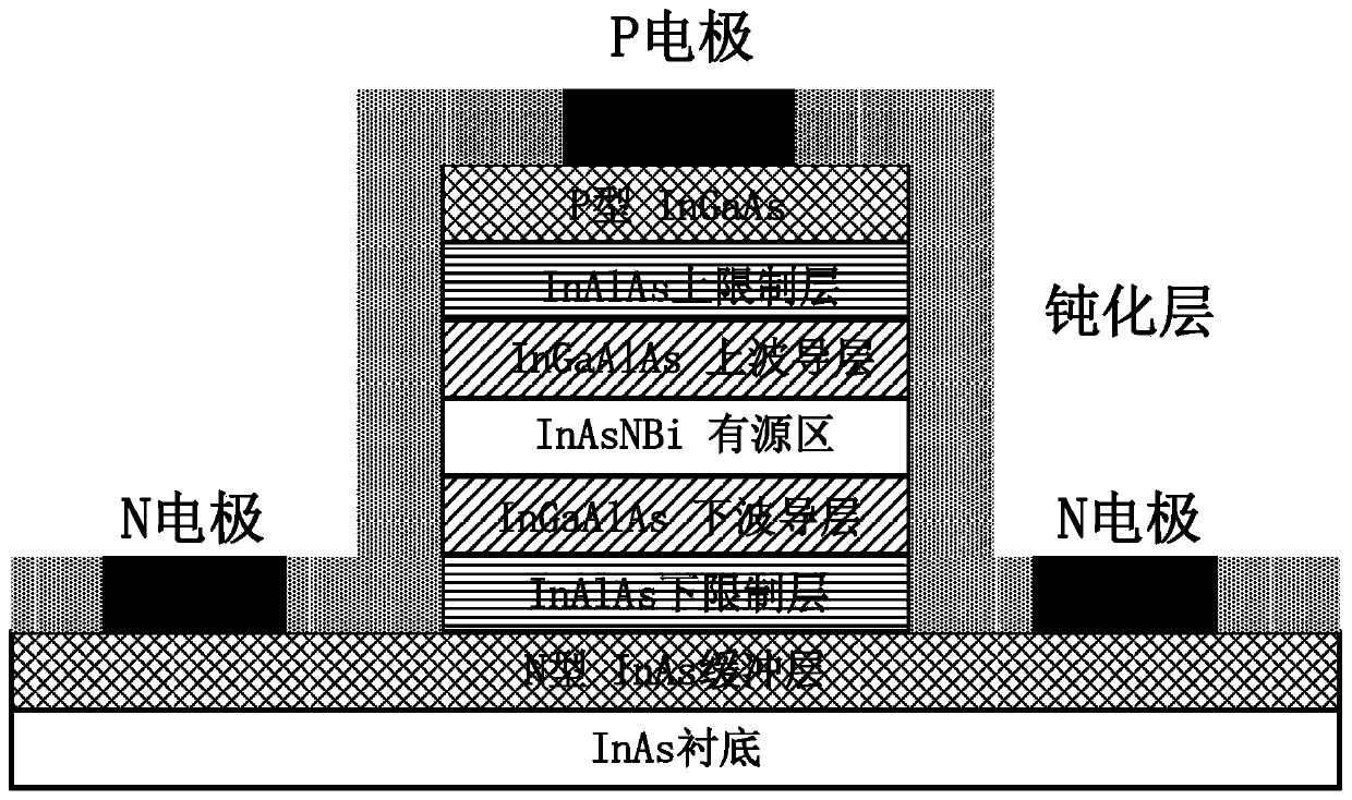
[0066] image 3 is provided according to an embodiment of the present application containing InAs 1-x-y N x Bi y Schematic diagram of the structure of a mid-infrared laser.

[0067] In this embodiment, an InAs buffer layer is epitaxially grown on an InAs substrate or an auxiliary substrate (template) using molecular beam epitaxy (MBE) or metal organic vapor deposition (MOCVD) epitaxial growth tools;

[0068] Epitaxial growth of InAs on the InAs buffer layer 1-x-y N x Bi y Thin films and heterojunction materials.

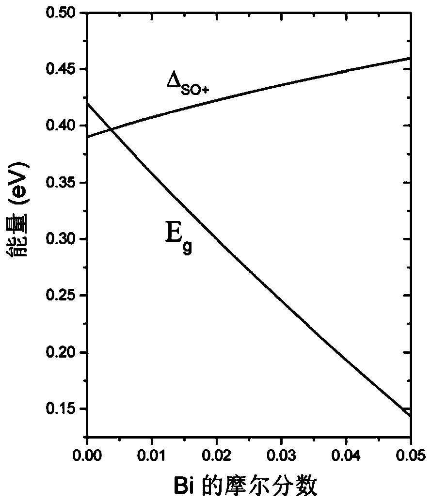
[0069] By controlling the concentration of doped In atoms and Bi atoms, the InAs 1-x-y N x Bi y The band gap of the material, the wavelength range can cover the mid-infrared.

[0070] The laser is a mid-infrared laser, which includes, in order from bottom to top: InAs substrate layer, N-type InAs buffer layer, InAlAs lower confinement layer, InGaAlAs lower waveguide layer, InAs 1-x-y N x Bi y Quantum well a...

Embodiment 2

[0089] Example 2: n-b-i-b-p type InAsNBi mid-infrared detector

[0090] The detector is a mid-infrared detector, which includes in order from bottom to top: InAs substrate, N-type InAs contact layer, N-type InAsNBi hole blocking layer, P-type InAs 1-x-y N x Bi y Absorbing layer, P-type InAsNBi electron blocking layer and P-type InAs contact layer,

[0091] Wherein, the outer surface of the N-type InAs contact layer, the N-type InAsNBi hole blocking layer, the P-type InAsNBi absorbing layer, the P-type InAsNBi electron blocking layer, and the P-type InAs contact layer A passivation layer is deposited,

[0092] An N electrode is photoetched on the N-type InAs contact layer, and a P electrode is photoetched on the P-type InAs contact layer.

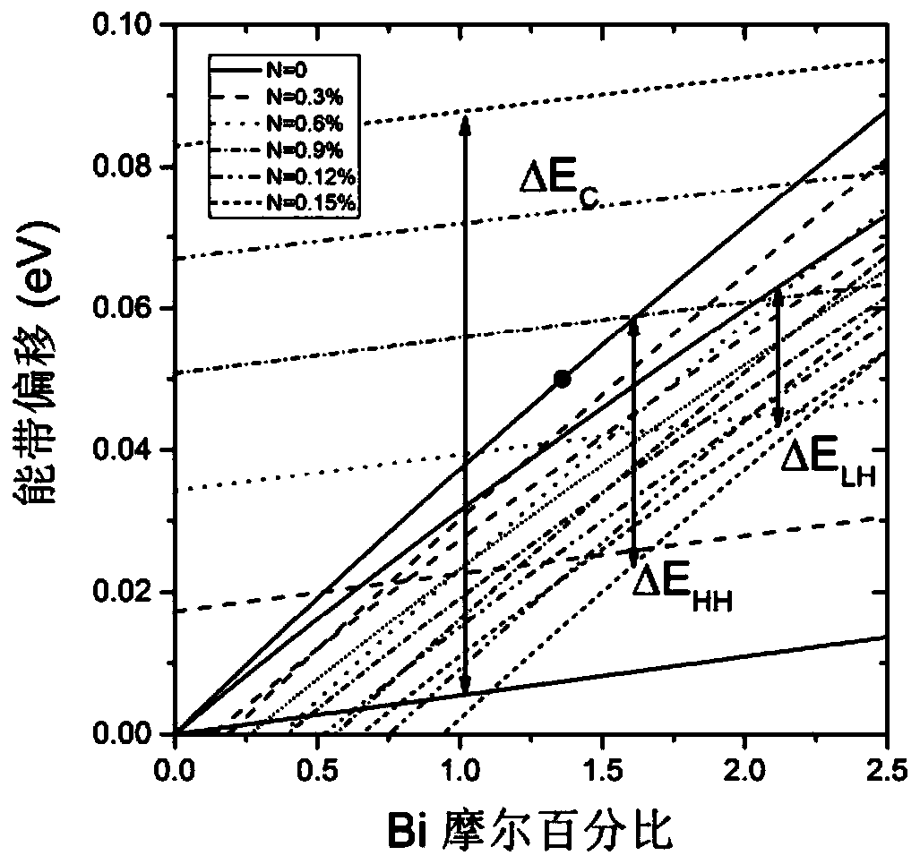
[0093] like Figure 4 As shown, the sphalerite-structured InAs 1-x-y N x Bi y The material has a forbidden band width of 0.22eV when N atoms are 4% and Bi atoms are 9.7%, and the corresponding wavelength is 5.64μm, which is located i...


PUM


Abstract

The invention discloses an indium-arsenic-nitrogen-bismuth semiconductor material, a laser using the material, a detector and a preparation method, and relates to the field of preparation of semiconductor photoelectric materials. The material comprises a substrate layer, a buffer layer and an indium-arsenic-nitrogen-bismuth semiconductor material. A certain concentration of Bi atoms and N atoms are doped in the InAs semiconductor in a co-doping manner, so that the forbidden bandwidth of the InAs material can be effectively adjusted, the coverage of the near-infrared-to-mid-infrared waveband can be realized, and the material is applied to an optoelectronic device. The doping of the Bi atoms enables the materials to grow more easily and more stably, and the introduction of N atoms can improve the solubility of Bi. In the InAs semiconductor, N atoms are doped at the same time, and the Bi atoms can effectively adjust the energy band structure of the compound. The material can grow by adopting various methods such as conventional molecular beam epitaxy, metal organic compound chemical vapor deposition and the like, and is simple in structure and operation process and easy to control.

Description

technical field [0001] The application relates to the field of semiconductor optoelectronic material preparation, in particular to an indium arsenic bismuth nitrogen semiconductor material, a laser and a detector using the material and a preparation method. Background technique [0002] Studies have shown that indium arsenide (InAs) in the III-V semiconductor family is a semiconductor material with excellent electrical properties. InAs materials have the advantages of large carrier concentration and high electron mobility. Adding a small amount of Bi atoms to InAs can reduce the band gap of the InAs material, and the rate of reduction of the band gap is about 40-50meV. InAsBi at room temperature 0.089 Compared with the InAs material, the bandgap value is reduced by 0.354eV. At the same time, InAs material as a direct bandgap semiconductor material can be used to construct type I and type II quantum wells, which makes InAs 1-x-y N x Bi y The material can be used as an al...

Claims


Application Information

Patent Timeline
IPC IPC(8): H01L31/0304H01L31/109H01L31/18H01S5/343
CPCY02P70/50
Inventor 芦鹏飞王凯林陆瑾张凡张丽王庶民
Owner 诺迪克(余姚)光电产业研究院有限公司
Why Eureka
Try Eureka