Array type narrow-band optical filter and preparation method thereof
A narrow-band filter and array technology, applied in filter, optics, optical components, etc., can solve the problems of high transmittance and narrow line width of plasmonic filter, poor out-of-band suppression, etc. , to achieve the effect of narrow line width, weak side peak and low cost
- Summary
- Abstract
- Description
- Claims
- Application Information
AI Technical Summary
Problems solved by technology
Method used
Image
Examples
Embodiment 1
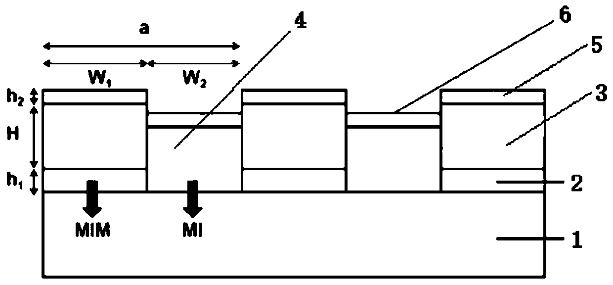
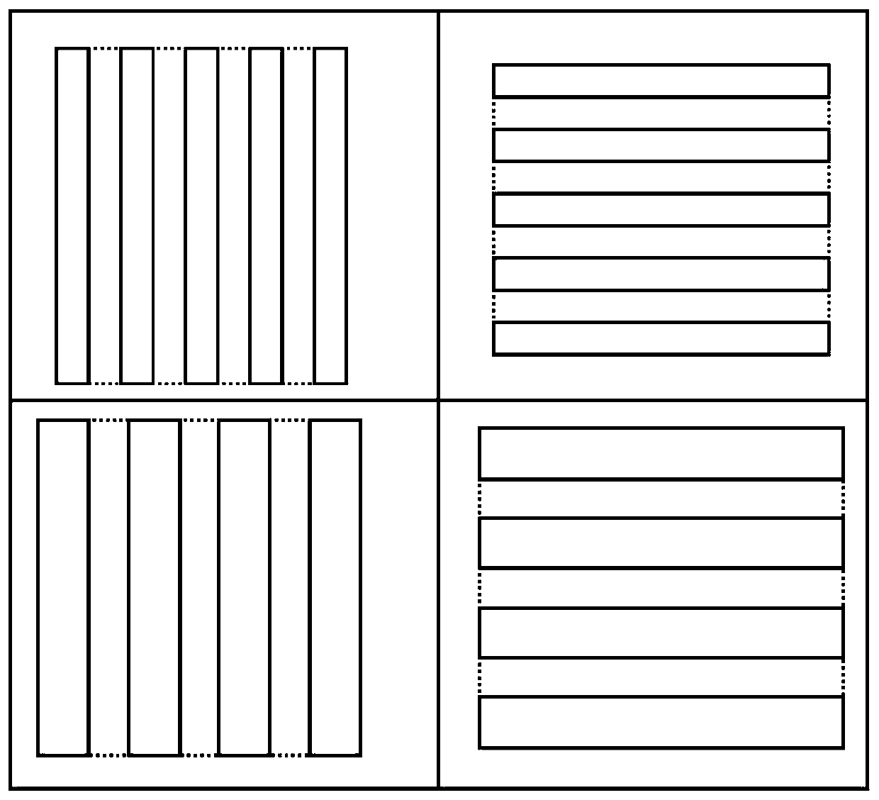
[0038] The invention provides an arrayed narrow-band optical filter, comprising a substrate (1) and a first grating and a second grating that are hybridized and nested on the substrate (1). In this embodiment, the first grating is a MIM grating. The second grating is an MI grating, and the MIM grating and the MI grating constitute a plasmonic composite grating, and the period of the plasmonic composite grating is the sum of the widths of the first grating and the second grating; the first grating is along the substrate (1) including the bottom metal layer (2), the dielectric layer (3), and the top metal layer (5) from bottom to top, and the second grating includes the dielectric layer (4) from bottom to top along the substrate (1) ), the top metal layer (6).
[0039] The materials of the two types of grating medium layers are the same as those of the substrate (1), and the materials of the metal layer are the same;
[0040] The period width of each group of plasmonic composit...
Embodiment 2
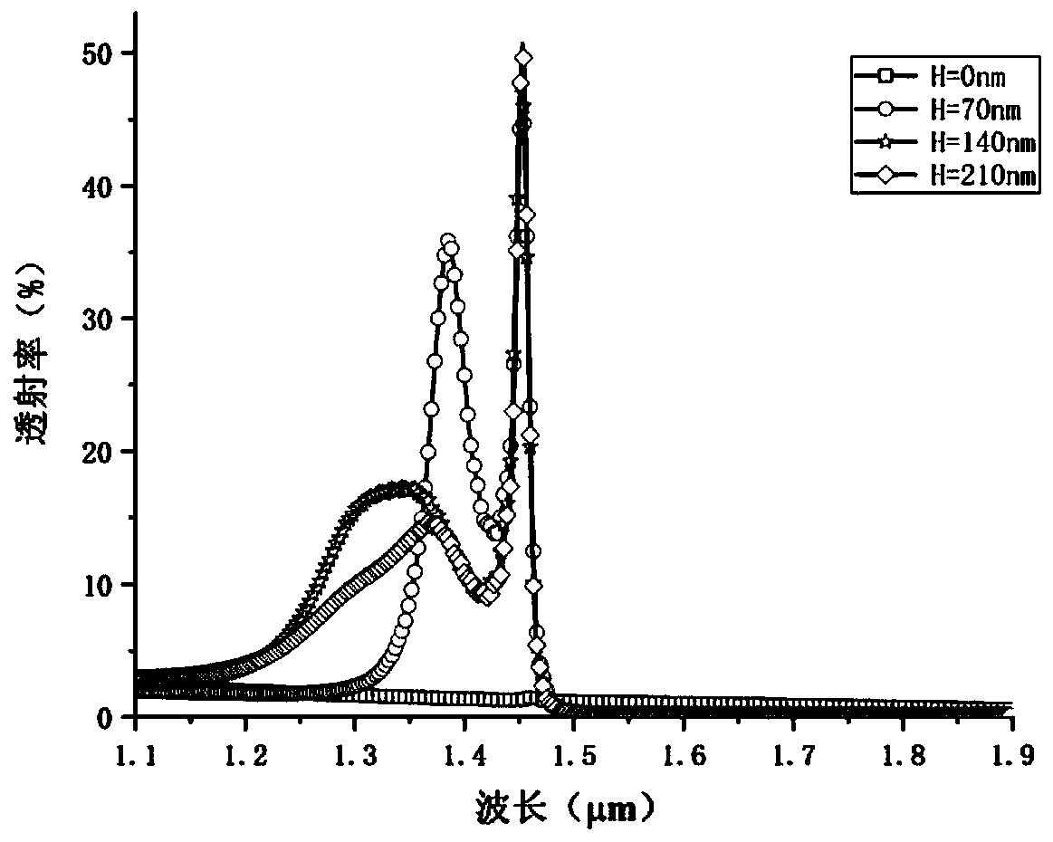
[0053] A preparation method of an array narrow-band optical filter. The finite difference-time domain (FDTD) algorithm and the surface plasmon dispersion relation are used to determine the period of a plasmon composite grating with a specific working center wavelength. The parameters such as the thickness of the dielectric layer and the ratio of the grating width are further tuned to achieve the required transmittance, bandwidth and side peak suppression, and the plasmonic composite grating structure is determined. Next, the preparation of the filter is finally completed using technologies such as UV lithography, laser direct writing, electron beam evaporation or magnetron sputtering coating, mask lift-off and reactive ion beam etching. Specifically include the following steps:
[0054] S1. Determine the period of the composite grating structure with a specific working center wavelength by using the finite time-domain difference algorithm and the surface plasmon dispersion rel...
Embodiment 3
[0068] S1. Determine the period of the composite grating structure with a specific working center wavelength by using the finite time-domain difference algorithm and the surface plasmon dispersion relationship, and further tune parameters such as the thickness of the dielectric layer and the ratio of the grating width to achieve the required transmittance, bandwidth and side peaks Suppression, to determine the parameters of the plasmonic composite grating;
[0069] Using Bragg coupling and surface plasmon wavenumber matching conditions, the transmission wavelength is calculated as follows:
[0070]
[0071] where λ is the central working wavelength;
[0072] ε m and ε d are the dielectric constants of metal and dielectric materials, respectively, and i is the harmonic resonance order;
[0073] S2: On the substrate (1), using ultraviolet lithography or laser direct writing processing technology, according to the specified working wavelength, the plasmon composite grating ...
PUM
| Property | Measurement | Unit |
|---|---|---|
| thickness | aaaaa | aaaaa |
Abstract
Description
Claims
Application Information


