Micron-sized diode chip and preparation method

A diode and micron-level technology, applied in electrical components, circuits, semiconductor devices, etc., can solve problems such as increased sidewall defects, reduced quantum efficiency in devices, and limitations in communication distance and practicability of micron LEDs, and achieve high output optical power , the effect of high response current and detection sensitivity

Active Publication Date: 2019-07-26
纳微朗科技(深圳)有限公司
View PDF6 Cites 8 Cited by
  • Summary
  • Abstract
  • Description
  • Claims
  • Application Information

AI Technical Summary

Problems solved by technology

The disadvantage of the second prior art is that the output light power of the micro-LED is relatively small, which limits the communication distance and practicability of the micro-LED; it etches the epitaxial wafer from the p-type layer to the n-type layer by dry etching, because Etching will increase the area of ​​the sidewall and increase the number of sidewall defects, which trap carriers in transport, resulting in a decrease in the internal quantum efficiency of the device

Method used


Image

  • Micron-sized diode chip and preparation method
  • Micron-sized diode chip and preparation method
  • Micron-sized diode chip and preparation method

Examples


Embodiment 1

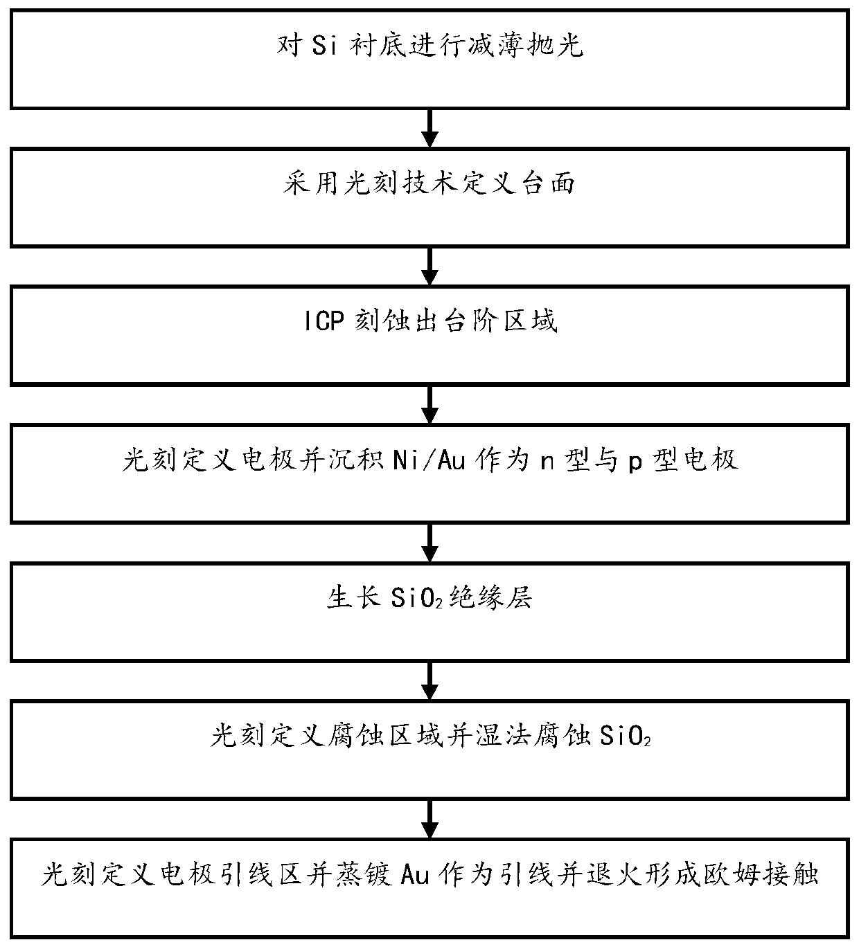
[0045] This embodiment provides a multi-functional micro-LED chip and its preparation method that restricts the carrier transport area by small-sized ITO, such as Figure 3-5 shown.

[0046] Taking the green light epitaxial wafer as an example, it specifically includes the following steps:

[0047] Step 1: From bottom to top, the sapphire substrate includes an unintentionally doped GaN layer of 3 microns, an n-GaN layer of 2 microns, a stress relief layer of 0.3 microns, a multi-quantum well light-emitting layer of 0.17 microns, a p-GaN layer of 0.5 microns, and ITO Electron transport layer; use S1818 photoresist at 4000 rpm, thickness of 1.8 microns to 2.2 microns, use UV photolithography machine (MA6) to expose for 10 seconds, use 0.5% NaOH solution to develop for 50 seconds;

[0048] Step 2: Use concentrated hydrochloric acid / concentrated nitric acid (4:1) mixed solution to corrode for 1 minute and 30 seconds;

[0049] Step 3: Using an Inductively Coupled Plasma Etcher (O...

Embodiment 2

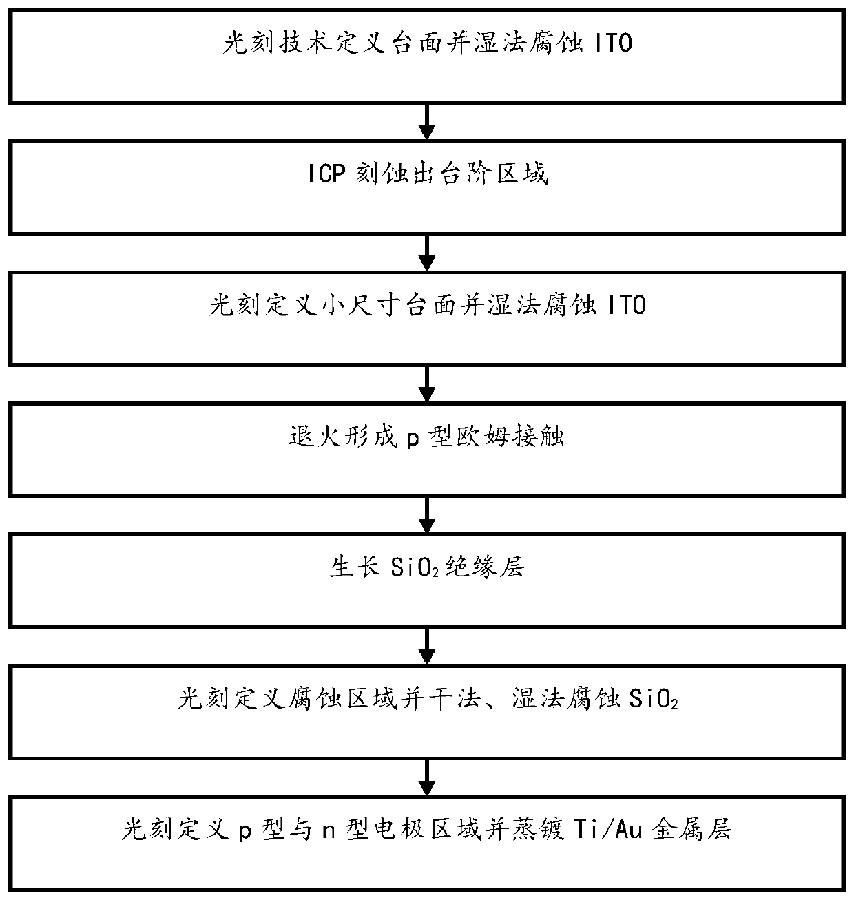
[0076] This embodiment provides a multifunctional micro-LED chip and its preparation method that activates magnesium doping of p-GaN by LEEBI (low-energy electron beam irradiation) to increase the carrier concentration in a limited area to limit the carrier transport area, such as Figure 3-5 shown.

[0077] Step 1: From bottom to top, the sapphire substrate includes an unintentionally doped GaN layer of 3 microns, an n-GaN layer of 2 microns, a stress relief layer of 0.3 microns, a multi-quantum well light-emitting layer of 0.17 microns, and a p-GaN layer of 0.5 microns; using S1818 photoresist at 4000 rpm, with a thickness of 1.8 microns to 2.2 microns, exposed for 10 seconds with a UV lithography machine (MA6), and developed with 0.5% NaOH solution for 50 seconds;

[0078] Step 2: Using an Inductively Coupled Plasma Etcher (Oxford), BCl 3 30sccm, Ar 15sccm, RF power 150 watts, ICP power 1000 watts, air pressure 10 mTorr, temperature 20 degrees Celsius, etching time 6 minu...


PUM


Abstract

The invention provides a micron-sized diode chip. The micron-sized diode chip comprises a first table surface, a second table surface, a gallium nitride layer, an n-GaN layer, a stress release layer,a multi-quantum-well light-emitting layer, a p-GaN layer, a first electrode, a second electrode and an insulating layer, wherein the sizes of the first table surface and the second table surface are different. The technical problems that an original LED is low in output light power and large in mismatch with GaN in thermal expansion rate and lattice constant are avoided; and the technical effectsof integration of multiple functions of communication, illumination, detection and the like on the same chip, and high light extraction efficiency are achieved.

Description

technical field [0001] The invention relates to the field of semiconductor optoelectronic devices, in particular to a multifunctional chip and its preparation Background technique [0002] The field of modern lighting has undergone four generations of changes, and LEDs have gradually entered the stage. LED has the advantages of energy saving, long life, environmental protection, strong robustness, controllability and durability. Since its invention, it has been applied in many aspects such as lighting, display, and optical communication. Among them, when used in the field of lighting, high-power characteristics of the device are required, and large-area LEDs are often used; GaN-based LEDs can emit blue and green light by changing the composition of quantum wells, and GaAs-based LEDs can emit red light. By integrating three-color LEDs It can realize full-color display, and covering light conversion materials such as phosphor powder or quantum dots on the surface of LED can a...

Claims


Application Information

Patent Timeline
Patent Type & Authority Applications(China)
IPC IPC(8): H01L33/00H01L33/06H01L33/32
CPCH01L33/0075H01L33/06H01L33/32H01L33/325
Inventor 田朋飞闫春辉周顾帆方志来张国旗
Owner 纳微朗科技(深圳)有限公司
Why Eureka
Try Eureka