Novel electroluminescent device and preparation method thereof

An electroluminescent device, a new type of technology, applied in the direction of electrical components, semiconductor devices, circuits, etc., can solve the problems of Joule heat dissipation, inability to effectively inject carriers, and limited tuning range, so as to improve the conductivity and achieve low Effects of Threshold Luminescence, Strong Locality and Field Enhancement Properties

Inactive Publication Date: 2019-08-16
NANJING UNIV OF AERONAUTICS & ASTRONAUTICS
View PDF3 Cites 11 Cited by
  • Summary
  • Abstract
  • Description
  • Claims
  • Application Information

AI Technical Summary

Problems solved by technology

As a semiconductor micro-nano light source, it is inevitable to face four problems: whether the carriers can be effectively injected; the improvement of the quality of the semiconductor micro-nano structure-based optical resonator; the suppression and regulation of the surface defec

Method used


Image

  • Novel electroluminescent device and preparation method thereof
  • Novel electroluminescent device and preparation method thereof
  • Novel electroluminescent device and preparation method thereof

Examples


Embodiment 1

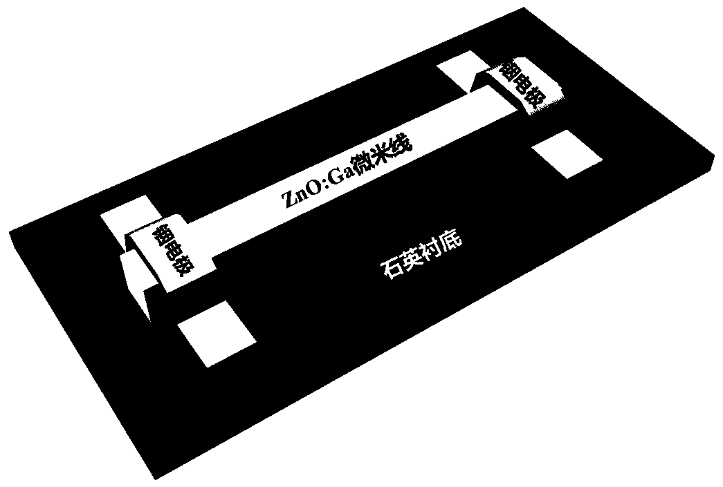
[0027] Such as figure 1 As shown, a new type of electroluminescent device includes quartz plates, ZnO:Ga micrometer wires, metal nanostructures, and indium electrodes arranged sequentially from bottom to top.

[0028] In the above structure, the size of the quartz plate is 3cm×2cm, the diameter of the ZnO:Ga microwire is 5-30μm and the length is 2cm, and the metal nanostructure is a metal nanostructure formed by annealing a gold / silver quasiparticle film. Particles.

[0029] The method for preparing the electroluminescent device described above includes the following steps:

[0030] (1) Substrate cleaning: Cut the quartz substrate into 3cm×2cm rectangular blocks, and cut the monocrystalline silicon into 3cm×1cm rectangular blocks, and use acetone, ethanol, and deionized water in an ultrasonic machine to clean them in order for 15 minutes. , Blow dry with nitrogen;

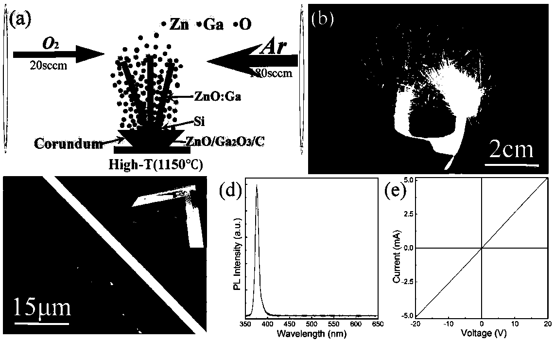
[0031] (2) ZnO:Ga micro-wires are prepared in a high-temperature tube furnace by chemical vapor deposition method, and...

Embodiment 2

[0035] Such as figure 1 As shown, a new type of electroluminescent device includes quartz plates, ZnO:Ga micrometer wires, metal nanostructures, and indium electrodes arranged sequentially from bottom to top.

[0036] In the above structure, the size of the quartz plate is 3cm×2cm, the diameter of the ZnO:Ga microwire is 5-30μm and the length is 2cm, and the metal nanostructure is a metal nanostructure formed by annealing a gold / silver quasiparticle film. Particles.

[0037] The method for preparing the electroluminescent device described above includes the following steps:

[0038] (1) Substrate cleaning: The quartz substrate is cut into 3cm×2cm rectangular blocks, and the single crystal silicon is cut into 3cm×1cm rectangular blocks, and the ultrasonic machine is washed with acetone, ethanol, and deionized water in order for 15 minutes. , Blow dry with nitrogen;

[0039] (2) ZnO:Ga micro-wires are prepared in a high-temperature tube furnace by chemical vapor deposition method, and...

Embodiment 3

[0045] Such as figure 1 As shown, a new type of electroluminescent device includes quartz plates, ZnO:Ga micrometer wires, metal nanostructures, and indium electrodes arranged sequentially from bottom to top.

[0046] In the above-mentioned structure, the size of the quartz plate is 3cm×2cm, the diameter of the ZnO:Ga micron wire is 5-30μm, and the length is 2cm. The metal nanostructure is composed of different plasmon resonance peaks synthesized by the seed method. Gold / silver nanospheres, nanorods or nano-biconical structures.

[0047] The method for preparing the electroluminescent device described above includes the following steps:

[0048] (1) Substrate cleaning: Cut the quartz substrate into 3cm×2cm rectangular blocks, and cut the monocrystalline silicon into 3cm×1cm rectangular blocks, and use acetone, ethanol, and deionized water in an ultrasonic machine to clean them in order for 15 minutes. , Blow dry with nitrogen;

[0049] (2) ZnO:Ga micro-wires are prepared in a high-t...


PUM

PropertyMeasurementUnit
Diameteraaaaaaaaaa
Lengthaaaaaaaaaa
Sizeaaaaaaaaaa

Abstract

The invention discloses a novel electroluminescent device and a preparation method thereof and belongs to the field of semiconductor optoelectronic devices. The invention provides the electroluminescent device based on a metal nanostructure/zinc oxide microwire composite structure. The device includes a Ga-doped ZnO microwire, a metal nanostructure, an indium electrode and a quartz wafer. The Ga-doped ZnO microwires prepared in the present invention have a diameter ranging from 5 to 30 micrometers and a length of up to 2 cm, Ga is selected as an effective donor doping source, an electroluminescent light source with different Ga doping concentrations and a tunable light-emitting center wavelength in the range of 500 nm to 650 nanometers by changing the mass ratio of a reaction source. Thanks to a strong local field enhancement effect of the metal nanostructure, the surface modification of the metal nanostructure is performed on ZnO:Ga microwires by physical sputtering and spin coating methods, the control of the light-emitting center wavelength and light-emitting area of the microwires is achieved, and therefore, a local-type point light source and an array light source with alternately red and green are prepared.

Description

Technical field [0001] The invention belongs to the field of semiconductor optoelectronic devices, and particularly relates to a novel electroluminescent device and a preparation method thereof. Background technique [0002] With the rapid development of photoelectric material preparation technology and characterization methods, the integration of optoelectronic functional devices is getting higher and higher, and the size of the devices is gradually approaching the physical limit. Therefore, the preparation of new micro-nano materials with controllable size, shape and composition and the research of micro-nano devices are particularly important. One-dimensional semiconductor micro-nano structures are considered to be one of the most ideal materials for integrated optoelectronic devices because of their superior optoelectronic properties, unique geometric structures, and natural side and end surfaces as resonant cavities. At the same time, compared with planar structures, semico...

Claims


Application Information

Patent Timeline
IPC IPC(8): H01L33/00H01L33/28
CPCH01L33/0033H01L33/0087H01L33/28H01L33/285
Inventor 阚彩侠冒王琪季姣龙姜明明
Owner NANJING UNIV OF AERONAUTICS & ASTRONAUTICS
Why Eureka
Try Eureka