
VO2-Sb film material with high speed and high data retention, and preparation method thereof
A technology of data retention and thin film materials, applied in the direction of electrical components, etc., can solve the problems of poor thermal stability of amorphous Sb thin films, and achieve the effects of low production cost, strong process controllability, and small component deviation
- Summary
- Abstract
- Description
- Claims
- Application Information
AI Technical Summary
Problems solved by technology
Method used
Image

Examples
preparation example Construction
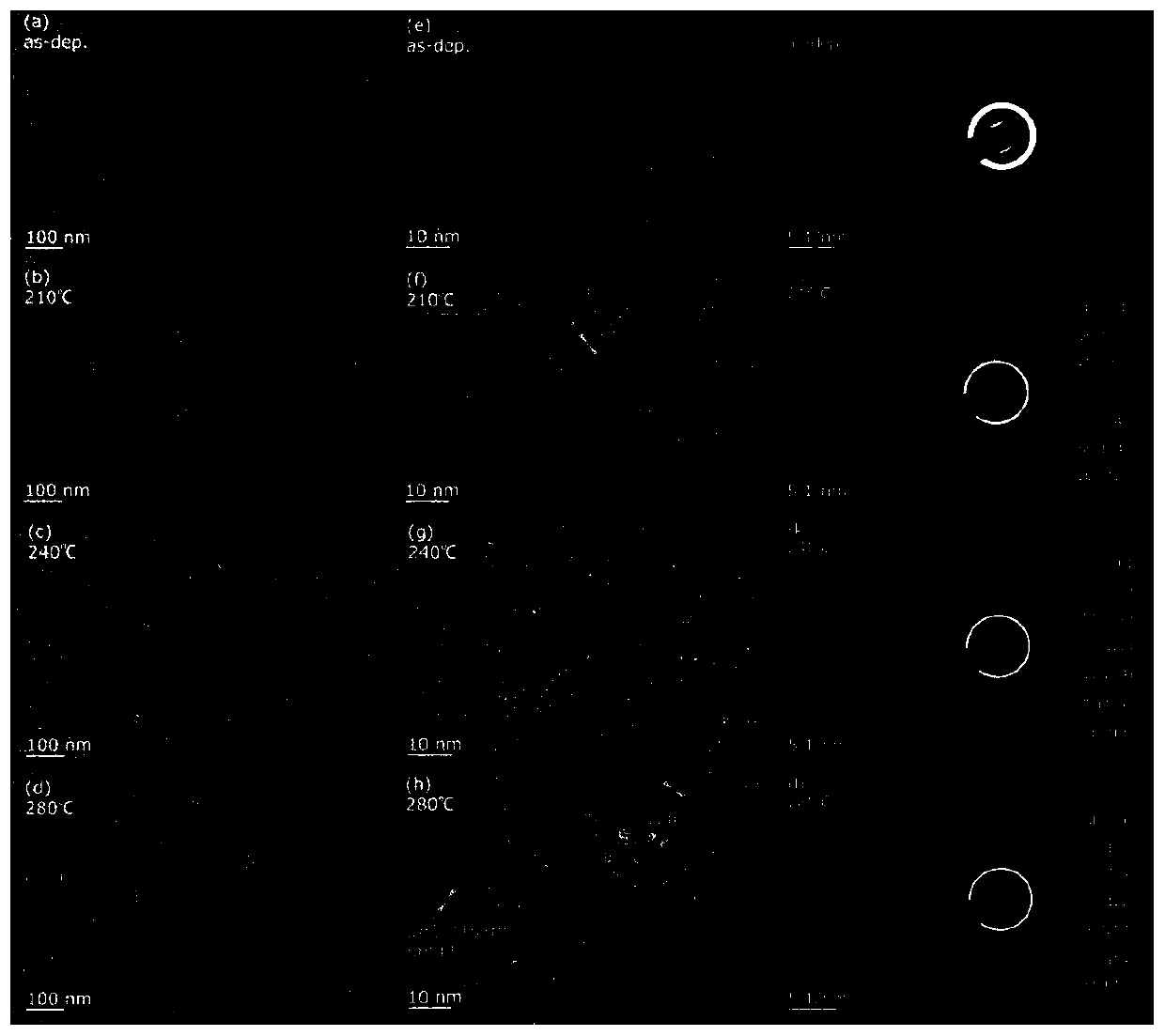
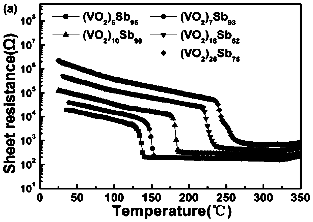
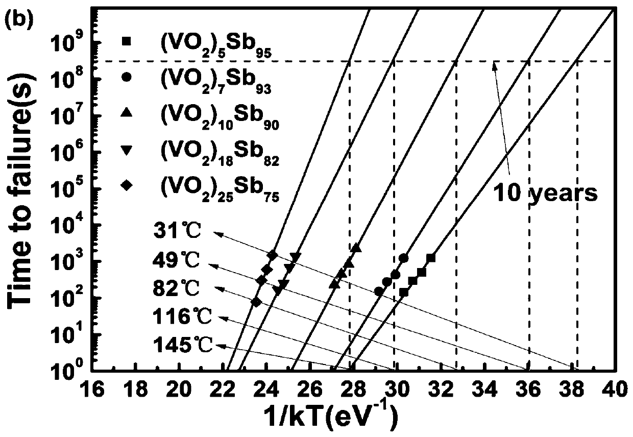
[0024] A vanadium dioxide-Sb thin film material with high speed and high data retention, whose chemical structure is (VO 2 ) x Sb 100-x , where VO 2 The atomic percentage content is 04 ~10 8 Ω, crystalline resistance 10 2 ~10 4 Ω. Its preparation method is as follows: using high-purity Sb simple substance and VO 2 As the target material, a magnetron sputtering device is used, a double-target co-sputtering method is adopted, high-purity argon is used as the working gas, and a quartz wafer or silicon wafer is used as the substrate material for surface deposition, and finally a transmission electron microscope is used to observe the microscopic structure, the specific steps are as follows:
[0025] (1) will VO 2 The target is installed in the magnetron DC sputtering target, and the Sb single substance target is installed in the magnetron RF sputtering target;
[0026] (2) Put the quartz wafer or silicon wafer substrate material into deionized water and absolute ethanol f...
Embodiment 1
[0033]A vanadium dioxide-Sb thin film material with high speed and high data retention, the preparation method of which is as follows:
[0034] (1) Using VO 2 Co-sputtering coating with Sb single target double target, VO 2 The target is installed in the magnetron DC sputtering target, and the Sb single target is installed in the magnetron RF sputtering target; the sputtering chamber is vacuumed, and when the vacuum degree in the sputtering chamber reaches 5×10 -4 Pa, fill the chamber with high-purity argon gas, the flow rate of argon gas is 50.0ml / min, until the glow pressure required for sputtering is 0.3Pa in the chamber; turn on the radio frequency power supply, and after the glow is stable, adjust the DC sputtering VO 2 The target power is 14 W, and the magnetron RF sputtering power of the Sb single target is 30 W. After the power is stable, turn on the substrate turntable and set the rotation rate to 5 rpm, open the baffle under the substrate, and sputter for 16 Minute...
Embodiment 2
[0038] Same as Example 1, the difference is that the magnetron radio frequency sputtering power of the Sb single substance target is 30W, and the DC sputtering VO 2 The target power is 17 W.
[0039] The Sb-VO prepared in above-mentioned embodiment 2 2 The film composition is measured by X-ray Energy Spectroscopy (EDS), and the film thickness is measured by a step meter. The test results are: the film composition is (VO 2 ) 7 Sb 93 , film thickness 100nm.
PUM
| Property | Measurement | Unit |
|---|---|---|
| crystallization temperature | aaaaa | aaaaa |
| thickness | aaaaa | aaaaa |
| thickness | aaaaa | aaaaa |
Abstract
Description
Claims
Application Information