Molybdenum sulfide/cesium lead halide perovskite quantum dot photoelectric detector and preparation method

A photodetector and molybdenum sulfide technology, which is applied in semiconductor/solid-state device manufacturing, photovoltaic power generation, electric solid-state devices, etc., can solve the problems of high cost, small application range, and low performance, and achieve low cost, wide application range, The effect of high sensitivity

Active Publication Date: 2019-08-30
QINGDAO TECHNOLOGICAL UNIVERSITY
View PDF11 Cites 8 Cited by
  • Summary
  • Abstract
  • Description
  • Claims
  • Application Information

AI Technical Summary

Problems solved by technology

[0005] The object of the present invention is to provide a two-dimensional molybdenum sulfide / cesium lead halide perovskite quantum dot composite nanostructure photodetector and its preparation method, aiming to solve the problem of molybdenum disulfide / semiconductor heterostructure photodetection in the prior art problems of high cost, low performance and small scope of application

Method used


Image

  • Molybdenum sulfide/cesium lead halide perovskite quantum dot photoelectric detector and preparation method
  • Molybdenum sulfide/cesium lead halide perovskite quantum dot photoelectric detector and preparation method
  • Molybdenum sulfide/cesium lead halide perovskite quantum dot photoelectric detector and preparation method

Examples


preparation example Construction

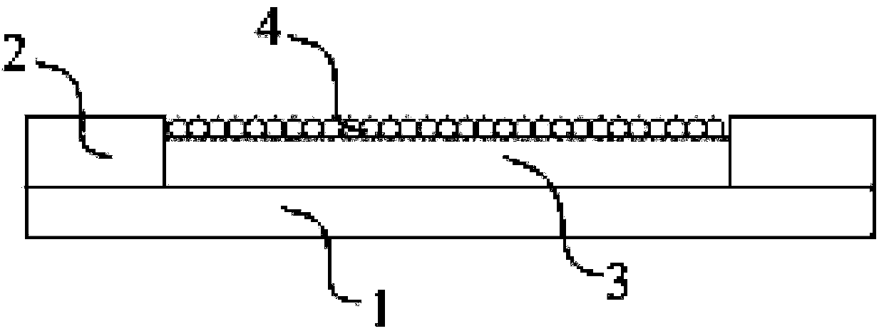
[0032] A preparation method of a two-dimensional molybdenum sulfide / cesium lead halide perovskite quantum dot composite nanostructure photodetector, comprising the following steps:

[0033] 1) take the substrate as the substrate layer, and make the surface electrodes separated from each other on the substrate layer;

[0034] 2) get the two-dimensional molybdenum sulfide thin film, and cover it on the substrate layer between the surface electrodes to obtain the two-dimensional molybdenum sulfide thin film layer;

[0035] 3) taking cesium lead-halogen quantum dots and uniformly covering them on the surface of the two-dimensional molybdenum sulfide thin film layer to obtain a cesium-lead-halogen quantum dot layer;

[0036] 4) get the ligand, add unsaturated fatty acid to get a mixed solution, the ratio of the ligand to the unsaturated fatty acid is 0.05-0.25mol / L; add a ligand solvent in the mixed solution to make a ligand solution, the mixed solution and The volume ratio of the...

Embodiment 1

[0044] A preparation method of a two-dimensional molybdenum sulfide / cesium lead halide perovskite quantum dot composite nanostructure photodetector, comprising the following steps:

[0045] 1) Take Si / SiO 2 The substrate, as the substrate layer, was fabricated on Si / SiO using photolithography 2 The desired electrode pattern is obtained on the substrate, and then the substrate is put into a vacuum coating system to perform vapor deposition of gold electrodes, and the thickness of the vapor deposition electrodes is 30 nm;

[0046] 2) Using polymethyl methacrylate as the carrier material, the two-dimensional molybdenum sulfide film is uniformly dispersed on the substrate between the two surface electrodes to obtain a two-dimensional molybdenum sulfide film layer;

[0047] 3) get the n-octane solution of cesium lead halogen quantum dots, the concentration is 50mg / mL, cover it evenly on the surface of the two-dimensional molybdenum sulfide thin film layer, carry out spin coating o...

Embodiment 2

[0053] A preparation method of a two-dimensional molybdenum sulfide / cesium lead halide perovskite quantum dot composite nanostructure photodetector, comprising the following steps:

[0054] 1) get mica sheet, as substrate layer, use photolithography to obtain required electrode pattern on this substrate, then this substrate is put into vacuum coating system to carry out vapor deposition silver electrode, and the thickness of vapor deposition electrode is 50nm;

[0055] 2) Using polymethyl methacrylate as the carrier material, spin coating a layer of polymethyl methacrylate on the molybdenum sulfide film by spin coating, and the spin coating speed is 2500 r / min. Baked for 10min; immersed in sodium hydroxide solution, heated for 30min; covered on the above-mentioned substrate layer, dried at 100°C, and cleaned to obtain a two-dimensional molybdenum sulfide thin film layer;

[0056] 3) Take the toluene solution of cesium lead halogen quantum dots with a concentration of 20 mg / mL,...


PUM


Abstract

The invention provides a molybdenum sulfide/cesium lead halide perovskite quantum dot photoelectric detector and a preparation method and relates to the technical field of a photoelectric detector. The photoelectric detector includes a substrate layer, and two surface electrodes separated from each other are arranged on the substrate layer; a two-dimensional molybdenum sulfide film layer is arranged on the substrate layer between the two surface electrodes, and a cesium lead halide quantum dot layer is further arranged on the two-dimensional molybdenum sulfide film layer. The invention furtherprovides a method of preparing the above photoelectric detector, the surface of the quantum dot film is modified by a ligand, and thereby preparation of the photoelectric detector is completed. The required electrodes are prepared on the substrate layer, a molybdenum sulfide nano film material is coated on a substrate, and the nano film material is covered with the cesium lead halide perovskite quantum dot film. The photodetector has the fast response speed, the response time is less than 100mus, high sensitivity and wide application range are achieved, the preparation method is simple, fastand efficient, simple and easy to operate, has low cost, is green and environmentally friendly and is suitable for large-scale production.

Description

technical field [0001] The invention relates to the technical field of electrical detectors, in particular to a two-dimensional molybdenum sulfide / cesium lead halide perovskite quantum dot composite nanostructure photoelectric detector and a preparation method thereof. Background technique [0002] Photodetectors are devices that convert optical signals into real-time electrical signals, and are an important part of optoelectronic systems. They are widely used in national defense, commercial, and scientific fields, and have an important impact on national defense technology and people's lives. With the rapid development of technology, traditional Si / SiO based 2 Various types of photodetectors of manufacturing technology are more and more difficult to meet the requirements of today's social development. Since the discovery of graphene in 2004, modern optoelectronic devices have extended into the emerging field of two-dimensional materials. With the birth of nanomaterials, s...

Claims


Application Information

Patent Timeline
Patent Type & Authority Applications(China)
IPC IPC(8): H01L51/42H01L51/48
CPCH10K30/10H10K30/00Y02E10/549
Inventor 米龙飞王攀
Owner QINGDAO TECHNOLOGICAL UNIVERSITY
Why Eureka
Try Eureka