Perovskite photovoltaic cell with potassium hexafluorophosphate film as interface passivation layer
A technology of potassium hexafluorophosphate and photovoltaic cells, applied in the field of materials, can solve the problems of rising cost, insufficient annealing temperature, etc., and achieve the effects of reducing preparation cost, low cost and high transmittance
- Summary
- Abstract
- Description
- Claims
- Application Information
AI Technical Summary
Problems solved by technology
Method used
Image
Examples
Embodiment 1
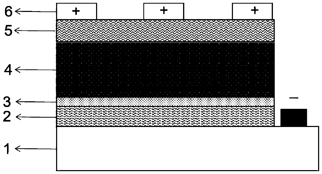
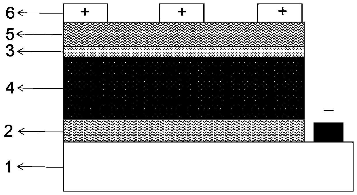
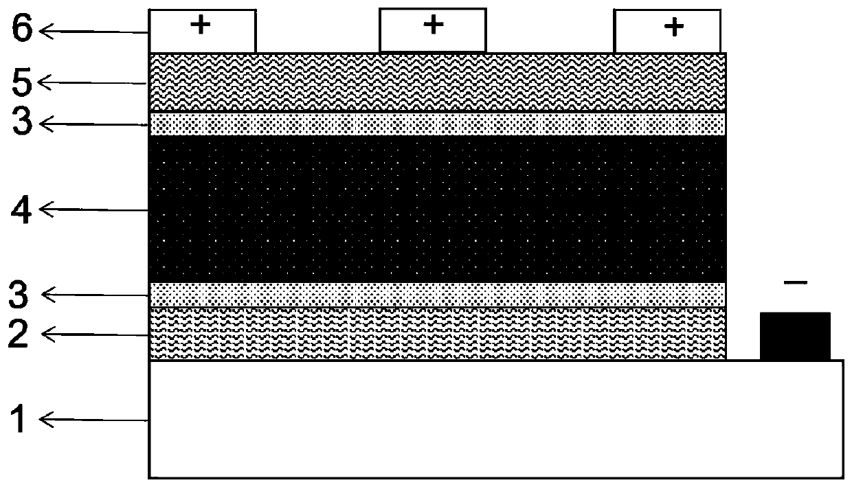
[0054] Such as figure 1 As shown, a planar perovskite photovoltaic cell includes a transparent conductive substrate 1, an electron transport layer 2, an interface passivation layer 3, a perovskite photosensitive active layer 4, a hole transport layer 5 and a metal electrode 6. The preparation method comprises the following steps:
[0055] (1) Treatment of transparent conductive substrate: cleaning FTO (fluorine-doped SnO 2 ) conductive glass sheet, first soak the conductive glass sheet in warm water filled with detergent (such as Libai brand liquid detergent) for 20 minutes, then rinse it with clean water after repeated scrubbing; then polish it with polishing powder; Then put them into containers containing deionized water, acetone and alcohol and sonicate them for 20 minutes respectively; finally put them into deionized water and rinse them twice, then dry them with a nitrogen gun and dry them in an oven at 80°C;
[0056] (2)SnO 2 Thin Film Fabrication: Fabrication of SnO...
Embodiment 2
[0067] Such as figure 1 As shown, a planar structure perovskite photovoltaic cell includes a transparent conductive substrate, an electron transport layer, an interface passivation layer, a perovskite photosensitive active layer, a hole transport layer and a metal electrode, and its preparation method includes the following steps:
[0068] (1) cleaning ITO conductive glass sheet: with embodiment 1;
[0069] (2)SnO 2 Thin Film Preparation: SnO Fabrication on ITO Substrates 2 film, and put it into a UV-ozone cleaner, and treat it with UV-ozone for 10 minutes in an atmospheric atmosphere and at room temperature, and the treated SnO 2 / ITO substrate is quickly transferred into the glove box;
[0070] (3) on SnO 2 Preparation of KPF on thin film 6 film;
[0071] a. Take 2.0mg of KPF 6 Particles were dissolved in 1 ml of ethyl acetate, completely dissolved before use;
[0072] b. Spin coating on SnO at a speed of 1000 rpm (15s) 2 QD film spin-coated KPF 6 solution to form...
Embodiment 3
[0078] Such as figure 1 As shown, a planar structure perovskite photovoltaic cell includes a transparent conductive substrate, an electron transport layer, an interface passivation layer, a perovskite photosensitive active layer, a hole transport layer and a metal electrode, and its preparation method includes the following steps:
[0079] (1) cleaning of the flexible transparent plastic substrate coated with ITO: with embodiment 1;
[0080] (2)SnO 2 Thin Film Fabrication: Fabrication of SnO on Flexible Transparent Plastic Substrates of ITO 2 QD thin film, and put it into the ultraviolet ozone cleaning instrument, treat with ultraviolet ozone at room temperature for 10 minutes in the atmosphere of the atmosphere;
[0081] (3) on SnO 2 Prepare KPF6 film on QD film;
[0082] a. Take 1mg of KPF 6 The granules were dissolved in 10 ml of ethyl acetate, completely dissolved before use;
[0083] b. Spin coating on SnO at a speed of 3000 rpm (15s) 2 Spin-coating KPF on QD fi...
PUM
 Abstract
Description
Claims
Application Information


