Ordered base al 1-x ga x Controllable epitaxial growth method of n quantum dots

An epitaxial growth, quantum dot technology, applied in electrical components, nanotechnology, circuits, etc., can solve the problems of difficult nanopillars and quantum dot distribution and structure control, achieve enhanced light extraction efficiency, facilitate large-scale processing, reduce cost effect

Active Publication Date: 2020-11-06
SUZHOU INST OF NANO TECH & NANO BIONICS CHINESE ACEDEMY OF SCI
View PDF4 Cites 0 Cited by
  • Summary
  • Abstract
  • Description
  • Claims
  • Application Information

AI Technical Summary

Problems solved by technology

[0005] In the current literature reports, when using MBE to selectively grow (controllable growth) nanopillar structures on GaN substrates, it often requires Focused ion beam (Focused ion beam, FIB) or electron beam lithography (E-beam lithography, EBL ) and other expensive and complicated processes; while self-assembly growth is still mainly used on Si substrates, which has a large randomness, and it is difficult to effectively control the distribution and structure of nanopillars and quantum dots.

Method used


Image

  • Ordered base al  <sub>1-x</sub> ga  <sub>x</sub> Controllable epitaxial growth method of n quantum dots
  • Ordered base al  <sub>1-x</sub> ga  <sub>x</sub> Controllable epitaxial growth method of n quantum dots
  • Ordered base al  <sub>1-x</sub> ga  <sub>x</sub> Controllable epitaxial growth method of n quantum dots

Examples


Embodiment 1

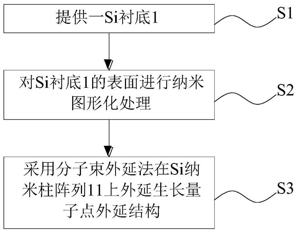
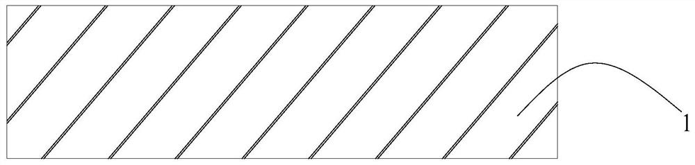
[0061] First, take a piece of Si substrate, wash the surface of Si substrate with acetone and ethanol solution for 10 minutes, and place it in an oxygen ion environment for 10 minutes to complete the hydrophilic treatment.

[0062] Then, a nano-patterning treatment is performed on the Si substrate by using a nano-sphere etching process.

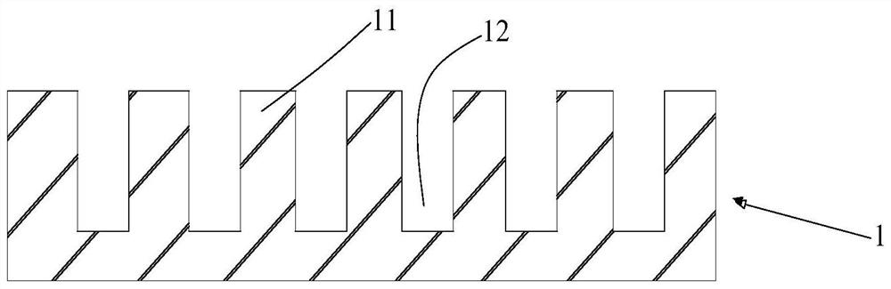
[0063] Specifically, in the first step, a layer of uniformly dispersed PS nanosphere film 1a is prepared on the surface of Si substrate 1 by self-assembly process, and the diameter of PS nanosphere is 500nm, such as Figure 10 As shown; the second step is to etch the PS nanospheres with oxygen plasma in the glue remover to reduce their diameter, and form a nanosphere mask 1b on the surface of the Si substrate 1, such as Figure 11 with Figure 14 Shown; the third step, use reactive ion etching (abbreviated as RIE) to etch the Si substrate 1 with nanosphere mask 1b for about 2min, and the Si substrate 1 between PS nanospheres is etched away t...

Embodiment 2

[0071] First, take a piece of Si substrate, wash the surface of Si substrate with acetone and ethanol solution for 10 minutes, and place it in an oxygen ion environment for 15 minutes to complete the hydrophilic treatment.

[0072] Then, a nano-patterning treatment is performed on the Si substrate by using a nano-sphere etching process.

[0073] Specifically, the first step is to prepare a uniformly dispersed PS nanosphere solution. The specific method is to use a micropipette to measure the PS nanosphere dispersion (10% by mass, and the diameter of the PS nanosphere is 200nm) and absolute ethanol The solution was placed in a small beaker, the volume ratio of the two was 1:2, and the solution was ultrasonically dispersed for 10 minutes to obtain a uniformly dispersed PS nanosphere solution; in the second step, PS nanospheres were pre-assembled on the water surface, specifically The method is to prepare a petri dish filled with deionized water (the surface area of ​​the water i...

Embodiment 3

[0082] First, take a piece of Si substrate, wash the surface of the Si substrate with acetone and ethanol solution for 12 minutes, and place it in an oxygen ion environment for 12 minutes to complete the hydrophilic treatment.

[0083] Then, a nano-patterning process is performed on the Si substrate by using a nano-imprint process.

[0084] Specifically, in the first step, a layer of embossing glue 1c is coated on the surface of Si substrate 1, such as Figure 18 As shown; the second step is to use a mold to transfer the nanometer pattern to the imprinting glue 1c, and its pattern is a round column arranged in a square, with a diameter of 50nm and a spacing of 200nm, and it is cured with an ultraviolet light source and placed on the Si substrate 1 Form the imprint glue mask 1d, such as Figure 19 Shown; the third step is to etch the Si substrate 1 with the imprinting rubber mask 1d by ICP, the etching depth is 400nm, and the Si substrate 1 between the imprinting rubber mask 1...


PUM

PropertyMeasurementUnit
thicknessaaaaaaaaaa
thicknessaaaaaaaaaa
thicknessaaaaaaaaaa

Abstract

The invention discloses an ordered Si-based Al 1‑x Ga x The controllable epitaxial growth method of N quantum dots comprises the steps of: S1, providing a Si substrate; S2, carrying out nano-patterning treatment on the surface of the Si substrate, the surface of the Si substrate is recessed inwardly to form a Si nano-column array, and The suppression layer is deposited at the bottom of the groove between the Si nanocolumn arrays; S3, the AlN buffer layer, the first GaN nanocolumn, Al 1‑x Ga x N quantum dot structure, and a second GaN nanocolumn and / or Al 1‑z Ga z N nanocolumns; wherein, 0<x<1, 0<z<1. According to the controllable epitaxial growth method of the present invention, on the one hand, the Si nanopillar array is used to realize the Al 1‑x Ga x The selective growth of the N quantum dot structure enhances the ability to control the size and distribution of the Si-based quantum dot structure. On the other hand, the support of the first GaN nanocolumn can also help release epitaxial stress and improve crystal quality.

Description

technical field [0001] The invention belongs to Al 1-x Ga x The field of N quantum dot manufacturing technology, specifically, relates to an ordered Si-based Al 1- x Ga x Controllable epitaxial growth method of N quantum dots. Background technique [0002] Gallium nitride (GaN) material has the advantages of wide band gap, high thermal conductivity, stable physical and chemical properties, and strong radiation resistance. Al in GaN material system 1-x Ga x The band gap of N (commonly known as aluminum gallium nitrogen) material is continuously adjustable, and its wavelength can cover the ultraviolet band of 200nm to 365nm. It is an ideal material for the preparation of ultraviolet light-emitting devices. The application market exceeds 10 billion; but currently Al 1-x Ga x N-ultraviolet light-emitting devices have not yet occupied the main market, because their light extraction efficiency (LEE) and internal quantum efficiency (Internal quantum efficiency, IQE) are lo...

Claims


Application Information

Patent Timeline
Patent Type & Authority Patents(China)
IPC IPC(8): H01L33/00H01L33/06H01L33/12H01L33/22H01L33/32B82Y40/00
CPCB82Y40/00H01L33/007H01L33/06H01L33/12H01L33/22H01L33/32
Inventor 赵宇坤陆书龙
Owner SUZHOU INST OF NANO TECH & NANO BIONICS CHINESE ACEDEMY OF SCI
Why Eureka
Try Eureka