
Aerogel thermal insulation structure broadband infrared detector and preparation method thereof

An infrared detector and aerogel technology, which is applied in the field of infrared detectors, can solve the problems of increasing the complexity of the device process, loss of infrared radiation information, and increasing the preparation cost, so as to achieve broadband imaging, reduce the preparation cost, and improve the finished product. rate effect

Pending Publication Date: 2020-02-14
SHANGHAI INST OF TECHNICAL PHYSICS - CHINESE ACAD OF SCI
View PDF1 Cites 2 Cited by
  • Summary
  • Abstract
  • Description
  • Claims
  • Application Information

AI Technical Summary

Problems solved by technology

In summary, the use of the microbridge structure will increase the complexity of the device process on the one hand. In order to form the microbridge, it is necessary to prepare additional sacrificial layers, support layers and passivation layers, and additional etching processes are required. If the height is high, The difficulty will increase, there will be a risk of bridge deck collapse, and the yield will decrease, thereby increasing the manufacturing cost; on the other hand, the resonant cavity formed by the micro-bridge structure has wavelength selectivity, and different heights need to be designed for detection of different wavelength bands. The resonant cavity is matched with it, and once the device is completed, its response band will be fixed to a relatively narrow range, and the actual target has infrared radiation in the whole band range, so the use of the micro-bridge structure will also lead to many useful effects to a certain extent. The loss of target infrared radiation information

Method used


Image

  • Aerogel thermal insulation structure broadband infrared detector and preparation method thereof
  • Aerogel thermal insulation structure broadband infrared detector and preparation method thereof

Examples


Embodiment 1

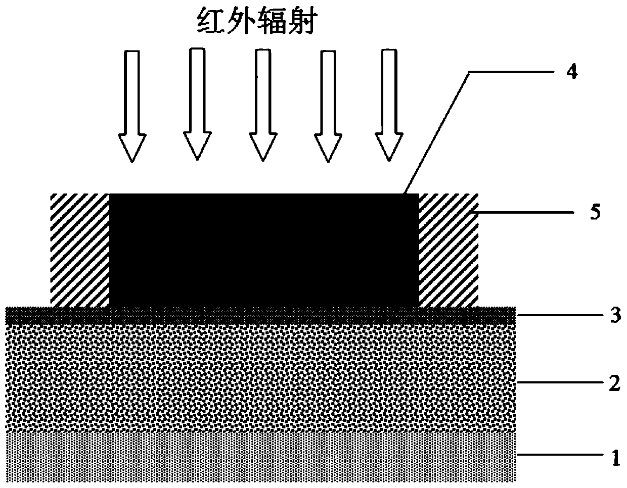
[0041] 1. Prepare a silica airgel film on a silicon wafer by a sol-gel method with a thickness of 2 μm.

[0042] 2. A silicon dioxide film is prepared on the silicon dioxide airgel film by magnetron sputtering, with a thickness of 50 nm.

[0043] 3. A manganese-cobalt-nickel-oxygen thermistor film was prepared on a silicon dioxide film by chemical solution deposition, with a thickness of 0.2 μm.

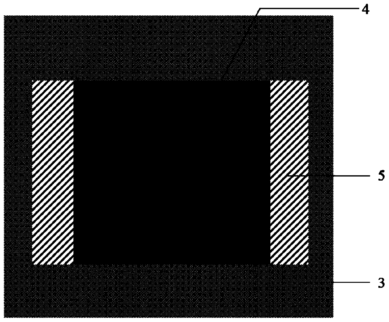
[0044] 4. Manganese-cobalt-nickel-oxygen thin-film detection elements are prepared on the manganese-cobalt-nickel-oxygen thermistor film through photolithography, corrosion, development and other photolithographic patterning processes. The area of ​​the detection element is 30 μm×30 μm.

[0045] 5. Through photolithography, corrosion, development and other photolithographic patterning processes, the dual ion beam sputtering method is used to prepare chromium and gold composite electrodes at both ends of the manganese-cobalt-nickel-oxygen thin film detector element, with a thickness o...

Embodiment 2

[0047] 1. Prepare a silica airgel film on a silicon wafer by a sol-gel method with a thickness of 3 μm.

[0048] 2. A silicon dioxide film is prepared on the silicon dioxide airgel film with a thickness of 100 nm by magnetron sputtering.

[0049] 3. A manganese-cobalt-nickel-oxygen thermistor film was prepared on a silicon dioxide film by magnetron sputtering, with a thickness of 0.6 μm.

[0050] 4. Manganese-cobalt-nickel-oxygen thin-film detection elements are prepared on the manganese-cobalt-nickel-oxygen thermistor film through photolithography, corrosion, development and other photolithographic patterning processes. The area of ​​the detection element is 50 μm×50 μm.

[0051] 5. Through photolithography, corrosion, development and other photolithographic patterning processes, the dual ion beam sputtering method is used to prepare chromium and gold composite electrodes at both ends of the manganese-cobalt-nickel-oxygen thin film detector element, with a thickness of 30nm a...

Embodiment 3

[0053] 1. Prepare a silica airgel film on a silicon wafer by a sol-gel method with a thickness of 5 μm.

[0054] 2. A silicon dioxide film was prepared on the silicon dioxide airgel film by magnetron sputtering, with a thickness of 150 nm.

[0055] 3. A manganese-cobalt-nickel-oxygen thermistor film was prepared on a silicon dioxide film by magnetron sputtering, with a thickness of 1 μm.

[0056] 4. Manganese-cobalt-nickel-oxygen thin-film detection elements are prepared on the manganese-cobalt-nickel-oxygen thermistor film through photolithography, corrosion, development and other photolithographic patterning processes. The area of ​​the detection element is 75 μm×75 μm.

[0057] 5. Through photolithography, corrosion, development and other photolithographic patterning processes, the magnetron sputtering method is used to prepare chromium and gold composite electrodes at both ends of the manganese-cobalt-nickel-oxygen thin film detector element, with a thickness of 30nm and 1...


PUM

PropertyMeasurementUnit
thicknessaaaaaaaaaa
thicknessaaaaaaaaaa
thicknessaaaaaaaaaa

Abstract

The invention discloses an aerogel thermal insulation structure broadband infrared detector and a preparation method thereof. The detector adopts a silicon wafer as a substrate, and is easy to be compatible with a modern silicon-based microelectronic processing technology. A silicon dioxide aerogel film is adopted as a thermal insulation layer, and a manganese-cobalt-nickel-oxygen thermistor filmwith broadband response characteristics is adopted as an infrared absorption layer. The device does not contain a traditional micro-bridge thermal insulation structure, the process is simple and easyto operate, a resonant cavity structure with a narrow response band cannot be formed, broadband detection can be realized, and more complete target infrared thermal radiation information can be obtained. In addition, the silicon dioxide aerogel thermal insulation layer has an overall supporting structure, the overall strength of the device is improved, the risk of bridge deck collapse possibly faced by a traditional micro-bridge structure does not exist, the yield is increased, and the preparation cost is reduced. The device and the preparation method thereof are mature in process and suitablefor unit, line array and area array infrared detectors.

Description

technical field [0001] The patent of the present invention relates to an infrared detector, specifically a wide-band thermistor film-type uncooled infrared detector based on an airgel heat insulation structure and a preparation method thereof. Background technique [0002] Uncooled infrared detectors do not require complex refrigeration systems, can work at room temperature, have the advantage of low cost, and have broad application prospects in both civilian and military fields, such as infrared thermal imaging, fire alarms, non-contact measurement Temperature, medical diagnosis, product production monitoring, missile early warning and interception and many other aspects. Among them, the thermistor-type infrared detector is a very important type of uncooled infrared detector. The basic principle is to detect the infrared heat radiation by measuring the change of the resistance of the heat-sensitive material caused by the target infrared heat radiation. The properties of th...

Claims


Application Information

Patent Timeline
Patent Type & Authority Applications(China)
IPC IPC(8): G01J5/20
CPCG01J5/20
Inventor 马建华黄志明褚君浩
Owner SHANGHAI INST OF TECHNICAL PHYSICS - CHINESE ACAD OF SCI
Learn More