
Dielectric passivation film for reducing electro-induced degradation of PERC battery and preparation method of dielectric passivation film
A technology of electric attenuation and passivation film, which is applied in the direction of circuits, photovoltaic power generation, electrical components, etc., can solve the problems that are not suitable for industrial mass production, the reduction effect is not obvious, and the technical difficulty is large, so as to achieve enhanced passivation effect, The effect of moderate technical difficulty and high compatibility
- Summary
- Abstract
- Description
- Claims
- Application Information
AI Technical Summary
Problems solved by technology
Method used
Image

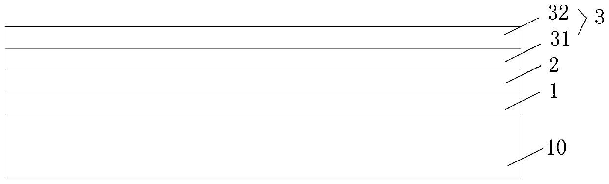
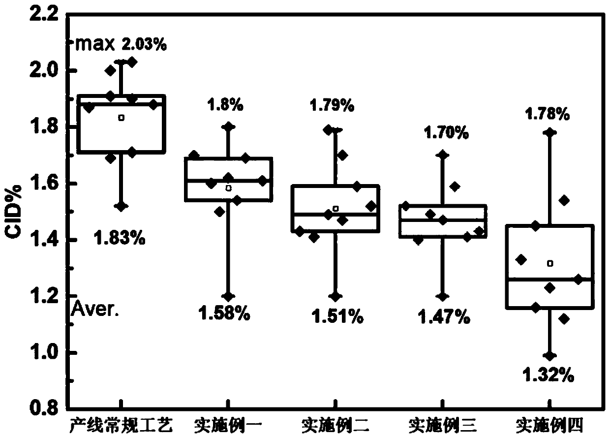
Examples
Embodiment approach
[0048] The refractive index of the first layer of SiNx is 2.20%-2.24%, and the refractive index of the second layer of SiNx is 2.16%-2.19%;
[0049] Alternatively, the refractive index of the first layer of SiNx is 2.18%-2.20%, and the refractive index of the second layer of SiNx is 2.12%-2.16%;
[0050] Alternatively, the refractive index of the first layer of SiNx is 2.16%-2.19%, and the refractive index of the second layer of SiNx is 2.10%-2.14%.
[0051] Further, the silicon oxide layer is carried out in a reaction chamber with a temperature of 385-420°C, a plasma power of 5000-6500W, a pressure of 800-1200mTor, and a deposition duty ratio of (1-3): (150)ms. The nitrous oxide flow rate is 4000-5000 sccm, the silane flow rate is 100-200 sccm, and the deposition time is 210s-250s. The silicon oxide passivation layer has good compactness, which can reduce the minority carrier recombination rate on the back surface of the silicon wafer, improve the open circuit voltage and sh...
Embodiment 1
[0066] P-type monocrystalline silicon wafer (10 -16 cm -1 ), after texturing, diffusion, SE laser, etching and normal pressure annealing, PERC coating on the back, including:
[0067] (1) Deposition of Al 2 o 3 1;
[0068] (2) Deposition of SiOx 2: The SiOx 2 process is carried out in a reaction chamber with a temperature of 400°C, a plasma power of 6000W, a pressure of 1000mTor, and a deposition duty ratio of 2:150ms. is 220s-240s;
[0069] (3) Deposition of the first layer of SiNx31: The process of the first layer of SiNx31 is carried out in a reaction chamber with a temperature of 420°C, a plasma power of 5500W, a pressure of 1600mTor, and a deposition duty ratio of 2:60ms, and the ratio of ammonia gas to silane is 3.6 :0.93, refractive index 2.18%-2.20%.
[0070] (3) Deposition of the second layer of SiNx32: The process of the second layer of SiNx32 is carried out in a reaction chamber with a temperature of 440°C, a plasma power of 5500W, a pressure of 1600mTor, and ...
Embodiment 2
[0072] P-type monocrystalline silicon wafer (10 -16 cm -1 ), after texturing, diffusion, SE laser, etching and normal pressure annealing, PERC coating on the back, including:
[0073] (1) Deposition of Al 2 o 3 1;
[0074](2) Deposition of SiOx 2: The SiOx 2 process is carried out in a reaction chamber with a temperature of 400°C, a plasma power of 6000W, a pressure of 1000mTor, and a deposition duty ratio of 2:150ms. is 220s-240s;
[0075] (3) Deposition of the first layer of SiNx31: The process of the first layer of SiNx31 is carried out in a reaction chamber with a temperature of 420°C, a plasma power of 5500W, a pressure of 1600mTor, and a deposition duty ratio of 2:60ms, and the ratio of ammonia gas to silane is 3.7 :0.90, refractive index 2.16%-2.19%.
[0076] (3) Deposition of the second layer of SiNx32: The process of the second layer of SiNx32 is carried out in a reaction chamber with a temperature of 440°C, a plasma power of 5500W, a pressure of 1600mTor, and a...
PUM
| Property | Measurement | Unit |
|---|---|---|
| refractive index | aaaaa | aaaaa |
| refractive index | aaaaa | aaaaa |
| refractive index | aaaaa | aaaaa |
Abstract
Description
Claims
Application Information