A groove composite multi-protrusion structure and its preparation process

A preparation process and recessed structure technology, applied in microstructure technology, microstructure devices, manufacturing microstructure devices, etc., can solve the problems of high cost and poor repeatability of the preparation process, and achieve the improvement of light absorption capacity and SERS activity. , the effect of improving Raman performance

Active Publication Date: 2020-09-22
JIANGSU HINOVAIC TECH CO LTD
View PDF1 Cites 0 Cited by
  • Summary
  • Abstract
  • Description
  • Claims
  • Application Information

AI Technical Summary

Problems solved by technology

[0004] The technical problem to be solved by the present invention is: the SERS activity enhanced by the microstructure of the existing disclosed SERS active substrate is not ideal enough, the existing preparation process has problems such as poor repeatability and high cost; the present invention provides a solution to solve the above problems A groove composite multi-protrusion structure and its preparation process

Method used


Image

  • A groove composite multi-protrusion structure and its preparation process
  • A groove composite multi-protrusion structure and its preparation process
  • A groove composite multi-protrusion structure and its preparation process

Examples


Embodiment 1

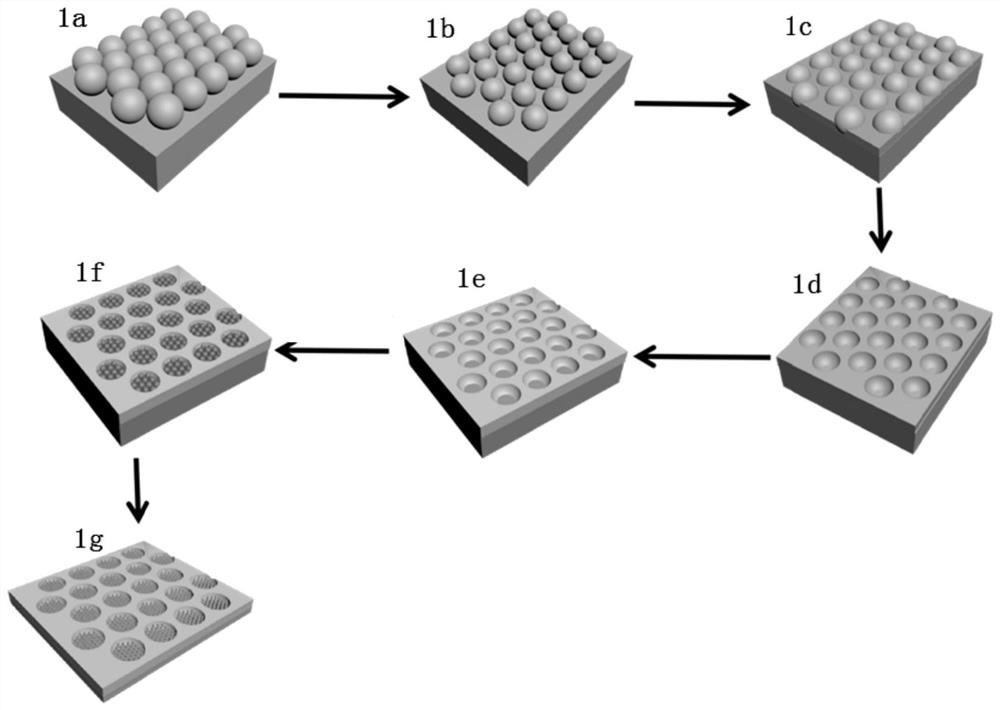
[0044] Example 1 - Fabrication of Groove Composite Multi-Protrusion Structure by Reactive Ion Etching Process

[0045] Step 1. Forming a silicon-based groove array structure

[0046] Step 1a, put the silicon wafer into deionized water, acetone, ethanol, concentrated sulfuric acid, hydrogen peroxide, and deionized water in sequence for ultrasonic cleaning, each liquid is ultrasonically cleaned for 30-40 minutes, and then the cleaned silicon wafer is dried at 120°C For treatment, the drying time is 20 minutes; after the water on the silicon wafer is completely evaporated, the silicon wafer is placed in an ultraviolet ozone cleaning machine for 30 minutes of irradiation to obtain a silicon wafer with a hydrophilic surface. Take 30 microliters of PS colloidal sphere suspension with a content of 2.5wt% and a diameter of 100 nm, mix it with ethanol in an equal volume, and then perform ultrasonic oscillation for 10 to 30 minutes, so as to obtain a uniformly dispersed ethanol dilution...

Embodiment 2

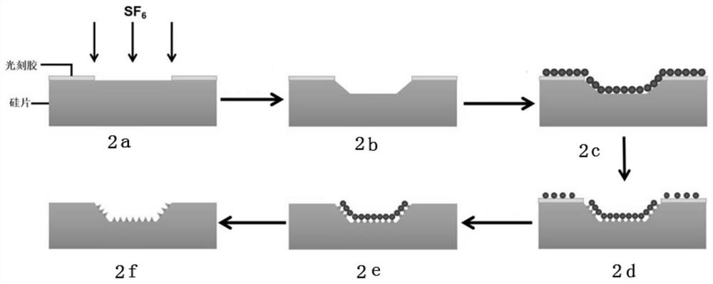
[0053] Example 2 - Preparation of groove composite multi-protrusion structure by photolithography technology combined with reactive ion etching process

[0054] The specific operation process of the photolithography process is in the prior art, and will not be repeated here. Due to the limitation of the lithography precision of the lithography instrument, the interval period width of the lithography mask plate during lithography is 10um. After constructing grooves with a width of 10 μm through the existing photolithography technology and reactive ion etching process, a 100 nm PS ball array was prepared by the same method as in step 1a of Example 1, and the above-mentioned obtained width of The 10um silicon-based groove array structure is compounded. After the above-mentioned silicon plate is naturally air-dried, the 100nm PS ball array is used as a secondary mask layer, and then the same process parameters as in the second etching of Example 1 are used for reactive ion etching...

Embodiment 3

[0055] Example 3 - Fabrication of Groove Composite Multi-Protrusion Structure by Reactive Ion Etching Process

[0056] Step 1. Forming a silicon-based groove array structure

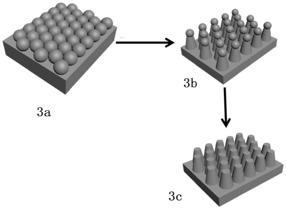
[0057] Step 1a, using the same method as step 1a in Example 1, respectively obtain a 100nm single-layer ordered hexagonal close-packed PS sphere array and a 500nm single-layer ordered hexagonal close-packed PS sphere array, such as Figure 6 Shown in a.

[0058] Step 1b, performing plasma etching on the 500nm single-layer ordered hexagonal close-packed PS sphere array prepared in step 1a, using oxygen as the working gas, controlling the gas flow at 30 sccm, maintaining the gas pressure at 3Pa, and controlling the etching power at 200W, and the total etching time is 40s at high-end or 3min at mid-range, so as to obtain a non-hexagonal close-packed PS ball array structure with a surface size of 350nm-450nm on the silicon wafer, such as Figure 6 Shown in b.

[0059] Step 1c, using the non-hexagonal clos...


PUM

PropertyMeasurementUnit
diameteraaaaaaaaaa
sizeaaaaaaaaaa
thicknessaaaaaaaaaa

Abstract

The invention discloses a groove composite multi-bulge structure and a preparation process thereof. The groove composite multi-bulge structure provided by the invention comprises a substrate, the semiconductor device further comprises a plurality of grooves arranged on the substrate, wherein the substrate is provided with a groove, the protrusions are compounded on the surface of the groove, the transverse size of the top of the groove is smaller than or equal to 1 micrometer, at least 1*105 grooves are formed in the substrate per square millimeter, the number of the protrusions compounded onthe surface of each groove is larger than or equal to 40, and the transverse size of the end, close to the surface of the groove, of each protrusion is larger than or equal to 60 nanometers. The SERSsubstrate is very novel in structure, and has high light absorption capacity and high SERS activity.

Description

technical field [0001] The invention relates to the field of surface-enhanced Raman spectroscopy (SERS) substrate materials, in particular to a groove composite multi-protrusion structure and a preparation process thereof. Background technique [0002] The SERS active substrate is usually prepared into several raised microstructures on the substrate, such as in a SERS substrate disclosed in CN104931480A and its preparation method, which adopts plasma bombardment of the substrate to prepare several raised microstructures, and then Then attach a layer of metal layer on the raised structure to make the SERS substrate. This structure increases the surface roughness due to the raised microstructure, thereby effectively enhancing the Raman scattering signal, but the enhanced SERS activity is not ideal enough, and further optimization and improvement of the microstructure is needed. [0003] Moreover, in the prior art, there are many methods for preparing the microstructure of SER...

Claims


Application Information

Patent Timeline
Patent Type & Authority Patents(China)
IPC IPC(8): B81B7/04B81C1/00G01N21/65
CPCB81B7/04B81C1/00055B81C1/00111B81C1/00119B81C1/00214B81C1/00523G01N21/65
Inventor 杨绍松毛海央刘广强陈大鹏
Owner JIANGSU HINOVAIC TECH CO LTD
Why Eureka
Try Eureka