A Schottky diode based on indium aluminum zinc oxide and its preparation method
A technology of Schottky diodes and oxides, which is applied in the manufacture of semiconductor/solid-state devices, semiconductor devices, electrical components, etc., can solve the problem of multi-element amorphous metal oxide semiconductor SBD research reports that are rare and easily affect IGZOSBD reverse leakage Current rectification performance, IGZOSBD is difficult to apply on a large scale and other issues, to achieve a wide bandgap modulation range, abundant storage, and ensure the effect of light stability
- Summary
- Abstract
- Description
- Claims
- Application Information
AI Technical Summary
Problems solved by technology
Method used
Image
Examples
Embodiment 1
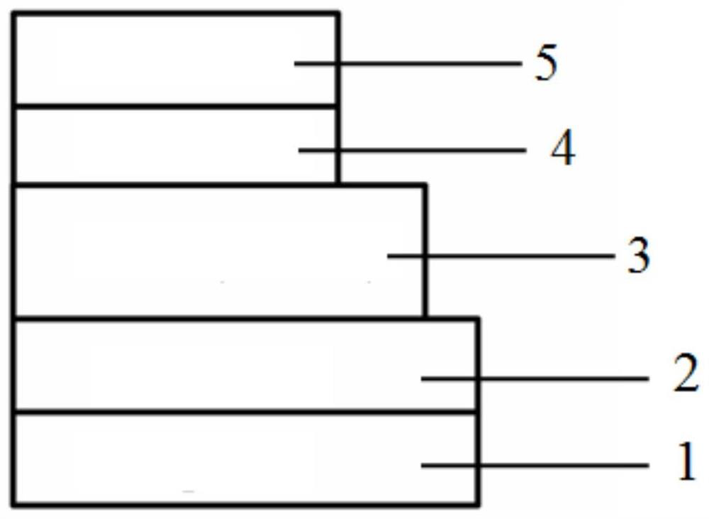
[0063] A Schottky diode based on Indium Aluminum Zinc Oxide, such as figure 1 As shown, the InAlZnO-based Schottky diode consists of SiO2 arranged sequentially from bottom to top 2 / P + -Si substrate 1, metal electrode Ti2, IAZO film 3 and double-layer metal electrode Pd, double-layer metal electrode Pd includes first layer metal electrode Pd4 and second layer metal electrode Pd5 arranged in sequence from bottom to top, IAZO film 3 It is an ohmic contact with the metal electrode Ti2, and it is a Schottky contact between the IAZO film 3 and the double-layer metal electrode Pd.
[0064] In the present invention, the band gap of the IAZO material is very wide and can be modulated in a wide range, which is beneficial to improving the stability of the performance of the IAZO SBD device under light. The metal electrode Ti2 is the cathode of the entire IAZO SBD. Ti has a low work function and can form a good ohmic contact with the IAZO film 3 to reduce the contact resistance and ob...
Embodiment 2
[0071] A kind of preparation method of the Schottky diode based on indium aluminum zinc oxide provided in embodiment 1, the steps include:
[0072] (1) on SiO 2 / P + - a metal electrode Ti2 is grown on the surface of the Si substrate 1, and Ti is used as a cathode;
[0073] In step (1), SiO 2 / P + -Si substrate 1 surface has been polished before use; Polished SiO 2 / P + - The Si substrate 1 is beneficial to ensure that each layer of film grown has a higher flatness. SiO 2 / P + - After the Si substrate 1 is polished, the substrate is cleaned with Decon cleaning agent, deionized water, acetone or isopropanol, and ethanol in sequence, and then blown dry with nitrogen. SiO 2 / P + - The cleaning of the Si substrate 1 after polishing can effectively improve the cleanliness of the substrate surface, which is conducive to improving the flatness of the film, reducing interface defects, and improving the performance of the IAZO SBD.
[0074] (2) grow IAZO thin film 3 on metal...
PUM
| Property | Measurement | Unit |
|---|---|---|
| thickness | aaaaa | aaaaa |
| thickness | aaaaa | aaaaa |
| thickness | aaaaa | aaaaa |
Abstract
Description
Claims
Application Information


