Method for inhibiting quantum dot surface defect state based on crystal face control

A technology of quantum dots and defect states, applied in the field of compound semiconductor nanomaterial preparation, can solve the problems of easy detachment of ligands on the surface of quantum dots, insufficient passivation of crystal planes, etc., and achieve the effects of improving optoelectronic performance, suppressing defect states, and effectively regulating

Inactive Publication Date: 2020-07-17
HUAZHONG UNIV OF SCI & TECH
View PDF1 Cites 2 Cited by
  • Summary
  • Abstract
  • Description
  • Claims
  • Application Information

AI Technical Summary

Problems solved by technology

[0006] The invention solves the problem that ligands on the surface of quantum dots in the prior art are easy to fall off, and is easily affected by the surrounding environment so that defects are introduced into the surface of quantum dots, and provides a method for suppressing defect states on the surface of quantum dots based on crystal plane control. Under the condition of high monomer concentration, the quantum dots are dominated by the kinetic growth mechanism and follow the anisotropic growth principle. The geometric structure of the obtained ~3nm quantum dots is approximately a regular octahedron, and the surface almost only contains {111} crystal planes.
This synthesis method can effectively solve the defect problem caused by insufficient passivation of {100} crystal facets, and can effectively improve its photoelectric performance.

Method used


Image

  • Method for inhibiting quantum dot surface defect state based on crystal face control
  • Method for inhibiting quantum dot surface defect state based on crystal face control
  • Method for inhibiting quantum dot surface defect state based on crystal face control

Examples


Embodiment 1

[0044] (1) Weigh 8.82g of zinc stearate, 0.45g of thioacetamide, and 100ml of ODE (1-octadecene) in a two-necked reaction flask. After vacuumizing the mixture, heat it to 140°C and keep it for 50min;

[0045] (2) Cool the product in a water bath to 50°C, add 4ml of n-octylamine, add ethanol after the solution is clarified, centrifuge, and wash twice to obtain ZnS quantum dots whose first excitation peak is 256nm;

[0046] (3) The cleaned ZnS quantum dots are respectively configured into two solutions with a higher concentration of 0.6mol / L and a lower concentration of 0.2mol / L, and the solvents are ODE;

[0047] (4) Weigh 2.919g of lead chloride and 35ml of oleylamine in another two-necked reaction flask, and heat the mixture to 140°C for 30min after vacuumizing the mixture;

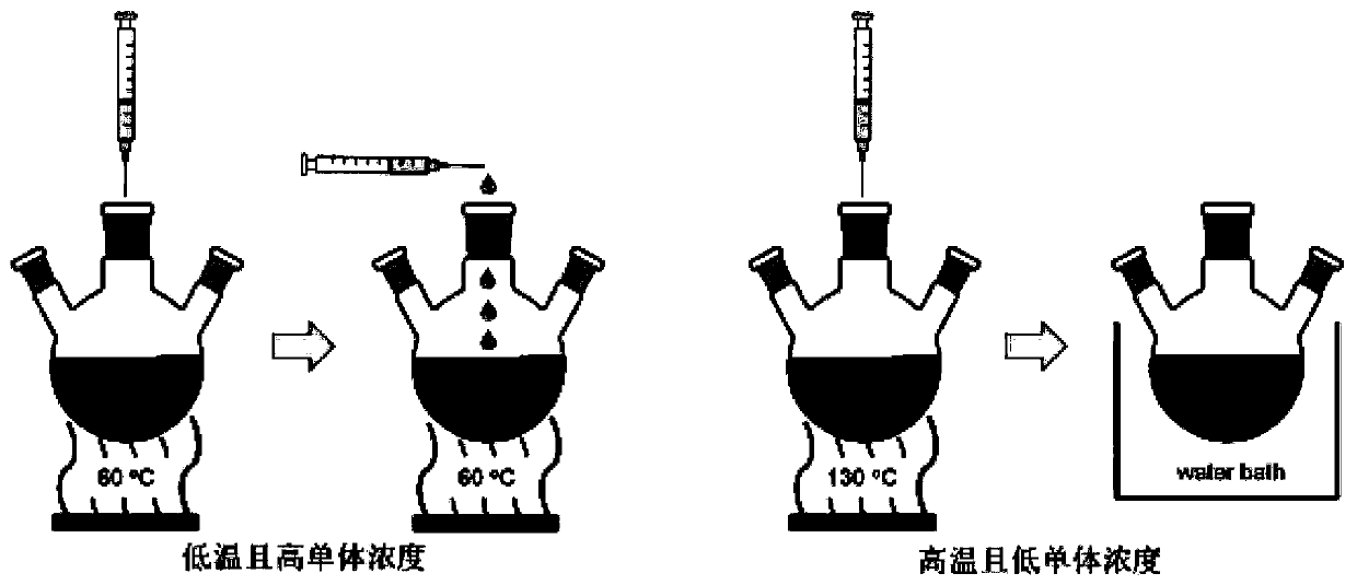
[0048] (5) Cool down to 60°C, quickly inject 5ml of ZnS quantum dot solution with a concentration of 0.6mol / L (the time of rapid injection should not exceed 1s, of course, the faster the better), and slo...

Embodiment 2

[0053] (1) The procedure for the preparation of ZnS quantum dots is the same as in Example 1. Weigh 3.336g of lead chloride and 40ml of oleylamine in one or two reaction bottles. After the mixture is evacuated, it is heated to 140°C and maintained for 30min;

[0054] (2) Cool down to 40°C, quickly inject 5ml of ZnS quantum dot solution with a concentration of 0.6mol / L, and slowly add ZnS quantum dot solution with a concentration of 0.2mol / L after 15s at a rate of about 0.04mmol / min, and start timing;

[0055] (3) Sampling is used to detect dimensional changes. At the 35th minute, the temperature is heated to 60°C, which can speed up the growth rate of quantum dots (of course, the temperature can be higher, and the maximum cannot exceed 120°C). Continue to detect dimensional changes through sampling, and inject at the 55th minute. Dilute with 60ml of n-hexane, inject 35ml of oleic acid as a ligand after the temperature drops to 40°C.

[0056] (4) adding a mixed solution of eth...

Embodiment 3

[0058] (1) The procedure for the preparation of ZnS quantum dots is the same as in Example 1. Weigh 2.502g of lead chloride and 30ml of oleylamine in one or two reaction flasks. After the mixture is evacuated, it is heated to 140°C and maintained for 30min;

[0059] (2) Cool down to 70°C, quickly inject 5ml of ZnS quantum dot solution with a concentration of 0.6mol / L, and slowly add ZnS quantum dot solution with a concentration of 0.2mol / L after 15s at a rate of about 0.04mmol / min;

[0060] (3) Sampling was used to detect the size change. After 28 minutes, water bath was injected into 40ml of n-hexane for dilution. After the temperature dropped to 40°C, 20ml of oleic acid was injected as a ligand.

[0061] (4) adding a mixed solution of ethanol and acetone for centrifugation, and removing the supernatant to obtain ~3nm PbS quantum dots prepared at low temperature.


PUM


Abstract

The invention discloses a method for inhibiting a quantum dot surface defect state based on crystal face control, and belongs to the technical field of preparation of compound semiconductor nano materials; the method includes heating the lead precursor solution to 40 DEG C to 70 DEG C, and then rapidly injecting a sulfur source or selenium source solution with the concentration of 0.6 mol / L to 0.8mol / L; slowly dropwise adding a sulfur source or selenium source solution with the concentration of 0.1 mol / L-0. 2mol / L; then adding a ligand, then adding an anti-solvent until the solution becomes turbid, then centrifuging, and precipitating to obtain lead sulfide quantum dots, lead selenide quantum dots, lead sulfide / lead selenide core-shell quantum dots or lead selenide / lead sulfide core-shellquantum dots which are wrapped by the ligand and have a body-centered tetragonal lattice structure, wherein the amount of substance of the lead precursor is greater than the sum of the amount of substance of the added sulfur source or selenium source, and the whole reaction is carried out under protective gas. The final product can effectively relieve the exposure condition of the {100} crystal face, avoids invasion of oxygen and moisture, has few surface defect states, and has good stability in air.

Description

technical field [0001] The invention belongs to the technical field of preparation of compound semiconductor nanomaterials, and more specifically relates to a method for suppressing surface defect states of quantum dots based on crystal plane control, in particular to a method for suppressing surface defect states of lead-based chalcogenide quantum dots based on crystal plane control Methods. Background technique [0002] Quantum dots are semiconductor nanomaterials whose optical and electrical properties are determined by their own size, shape and material composition. The size of quantum dots in three dimensions is less than 100nm, smaller than the Bohr radius of excitons, and will be bound in three spatial directions to be confined in the nanometer space. The internal electron and hole transport will be restricted, the mean free path of the electron is very short, the locality and coherence of the electron are enhanced, resulting in a quantum confinement effect, and the ...

Claims


Application Information

Patent Timeline
IPC IPC(8): C09K11/02C09K11/66C09K11/88B82Y20/00B82Y30/00
CPCB82Y20/00B82Y30/00C09K11/02C09K11/025C09K11/661C09K11/881
Inventor 张建兵王康夏勇连霖源张道礼唐江
Owner HUAZHONG UNIV OF SCI & TECH
Why Eureka
Try Eureka