Synaptic transistor based on two-dimensional and three-dimensional perovskite composite structure and preparation method of synaptic transistor

A composite structure and transistor technology, applied in semiconductor/solid-state device manufacturing, electric solid-state devices, semiconductor devices, etc., can solve problems such as limiting device performance, gate voltage failure, and difficulty in obtaining high-performance three-terminal synaptic transistors, etc., to achieve Avoid ion shielding effect, rapid migration effect

Active Publication Date: 2020-09-04
XIDIAN UNIV
View PDF6 Cites 5 Cited by
  • Summary
  • Abstract
  • Description
  • Claims
  • Application Information

AI Technical Summary

Problems solved by technology

[0004] However, the current research on three-terminal transistor-type synaptic devices based on halide perovskites is very lacking, and there are no reports on three-terminal perovskite synaptic transistors at home and abroad.
The main problem of three-terminal perovskite synaptic transistors is that the ion migration behavior in halide perovskite materials limits the device performance
For example, due to the ionic semiconductor characteristics of perovskite, ...

Method used


Image

  • Synaptic transistor based on two-dimensional and three-dimensional perovskite composite structure and preparation method of synaptic transistor
  • Synaptic transistor based on two-dimensional and three-dimensional perovskite composite structure and preparation method of synaptic transistor
  • Synaptic transistor based on two-dimensional and three-dimensional perovskite composite structure and preparation method of synaptic transistor

Examples


Embodiment 1

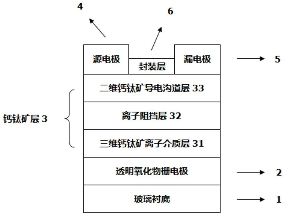
[0044] Embodiment 1: making FTO oxide gate electrode and Al 2 o 3 Purely inorganic three-dimensional perovskite synaptic transistors with an ion barrier.

[0045] Step 1: Treat the conductive substrate.

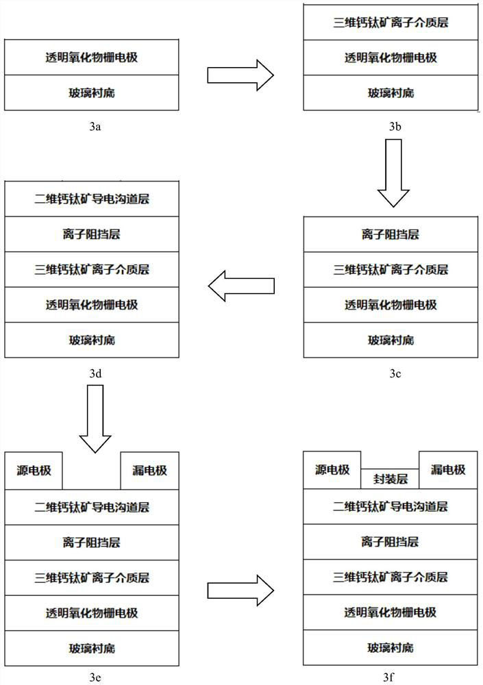
[0046] Such as image 3 As shown in a, the conductive substrate is composed of a substrate including a glass substrate and an FTO transparent oxide gate electrode. The conductive substrate is first cleaned with acetone, ethanol, and deionized water for 15 minutes ultrasonically, and then cleaned with a high-purity Drying with nitrogen gas; and then UV-ozone ultraviolet ozone treatment on the surface of the cleaned conductive substrate for 20 minutes to obtain the gate electrode of the synaptic transistor.

[0047] Step 2: Growing the perovskite region.

[0048] 2.1) If image 3 As shown in b, on the surface of the conductive substrate after ultraviolet ozone treatment, first spin-coat PbBr at a concentration of 1mol / L and a rotation speed of 2000r / min. 2 DMF solution fo...

Embodiment 2

[0055] Embodiment 2: making ITO oxide gate electrode and MoO 3 Organic-inorganic hybrid three-dimensional perovskite synaptic transistors with ion-blocking layers.

[0056] Step 1: Treat the conductive substrate.

[0057] Such as image 3 As shown in a, the conductive substrate is composed of a substrate including a glass substrate and an ITO transparent oxide gate electrode. The conductive substrate is first ultrasonically cleaned with acetone, ethanol, and deionized water for 15 minutes, and then cleaned with a high-purity Drying with nitrogen gas; and then UV-ozone ultraviolet ozone treatment on the surface of the cleaned conductive substrate for 20 minutes to obtain the gate electrode of the synaptic transistor.

[0058] Step 2: growing the perovskite region.

[0059] 2a) if image 3 As shown in b, on the surface of the conductive substrate after ultraviolet ozone treatment, spin-coat PbI at a concentration of 1.4mol / L and a rotation speed of 3000r / min. 2 DMF solution...

Embodiment 3

[0066] Embodiment 3: making FTO oxide gate electrode and Al 2 o 3 Organic-inorganic hybrid three-dimensional perovskite synaptic transistors with ion-blocking layers.

[0067] Step A: Treating the conductive substrate.

[0068] The specific implementation of this step is the same as step 1 of Embodiment 1.

[0069] Step B: Growing Perovskite Regions.

[0070] B1) If image 3 As shown in b, on the surface of the conductive substrate after ultraviolet ozone treatment, spin-coat PbI at a concentration of 1.4mol / L and a rotation speed of 3000r / min. 2 DMF solution for 45s to obtain PbI 2 layer; then in PbI 2 The layer was spin-coated with CH at a concentration of 100mg / mL and a rotation speed of 3000r / min. 3 NH 3I isopropanol solution for 45 s, and thermal annealing for 10 min under a nitrogen atmosphere at a temperature of 100 °C to obtain a three-dimensional CH with a thickness of 500 nm 3 NH 3 PB 3 ionic medium layer;

[0071] B2) If image 3 As shown in c, Al is gr...


PUM

PropertyMeasurementUnit
Thicknessaaaaaaaaaa
Thicknessaaaaaaaaaa
Thicknessaaaaaaaaaa

Abstract

The invention discloses a synaptic transistor based on a two-dimensional and three-dimensional perovskite composite structure and a manufacturing method of the synaptic transistor, and mainly solves the problem that an existing two-terminal perovskite synaptic device is inaccurate in synaptic behavior simulation. The synaptic transistor comprises a glass substrate (1), a transparent oxide gate electrode (2), a perovskite mining area (3), a source electrode (4), a drain electrode (5) and a packaging protection layer (6) from bottom to top. An ion dielectric layer is made of a three-dimensionalperovskite material, and a conductive channel layer is made of a two-dimensional perovskite material; carrier transport in the two-dimensional perovskite material is simulated by utilizing an electricfield formed by ion migration in the three-dimensional perovskite material; a device grid simulates a synaptic front film as an input end; and a device source and drain simulate a synaptic back filmto read current after synapsis. According to the invention, the two processes of carrier transport and grid control can be adjusted at the same time, regulation and control of source and drain currents are realized, the accuracy of synaptic behavior simulation of the synaptic transistor is improved, and the synaptic transistor can be used for simulating human neural synapses and constructing a neural network system.

Description

technical field [0001] The invention belongs to the technical field of semiconductor devices, and in particular relates to a synapse transistor and a preparation method thereof, which can be used to simulate human synapse and construct a neural network system. Background technique [0002] Emerging technologies such as artificial intelligence, big data, and the Internet of Things based on data information are profoundly changing human life and leading humans into the era of intelligent information. However, in the face of ever-expanding data information, traditional computers have long been unable to meet the needs of flexible processing and storage of large amounts of information due to the physical separation of computing units and memory, that is, the von Neumann bottleneck. How to improve the efficiency of storage and computing has become a difficult problem that human beings have to face. In contrast, the highly parallel nonlinear information processing capability of t...

Claims


Application Information

Patent Timeline
IPC IPC(8): H01L51/05H01L51/30H01L51/40
CPCH10K71/12H10K85/30H10K10/46Y02P70/50
Inventor 陈大正张春福田百川庞商政朱卫东樊刚张进成郝跃
Owner XIDIAN UNIV
Why Eureka
Try Eureka