Vertical double-heterojunction optical detector area array and manufacturing method thereof
A double heterojunction and photodetector technology, which is applied in the direction of electric solid-state devices, semiconductor devices, radiation control devices, etc. To achieve good semiconductor compatibility and system integration, improve photoresponsivity and response time, and high signal-to-noise ratio of area arrays
- Summary
- Abstract
- Description
- Claims
- Application Information
AI Technical Summary
Problems solved by technology
Method used
Image


Examples
no. 1 example
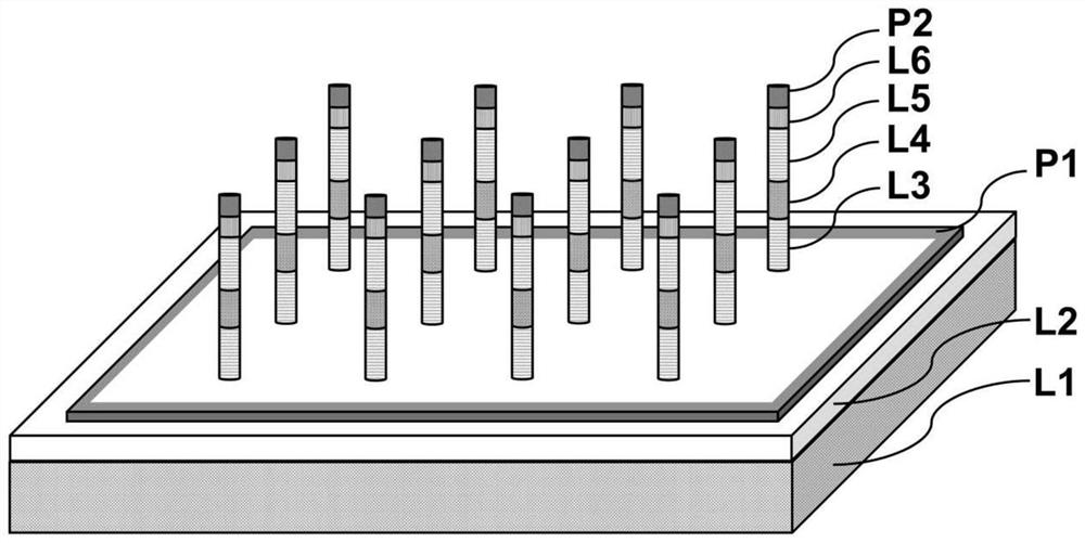
[0045] see figure 1, this embodiment provides a vertical double heterojunction photodetector array, the vertical double heterojunction photodetector array includes a transparent substrate L1, a lower ohmic contact layer L2 is arranged on the transparent substrate L1, and the lower ohmic contact layer A plurality of cylindrical double heterojunction detector units are arranged on L2, and the plurality of cylindrical double heterojunction detector units are arranged in an orderly manner on the lower ohmic contact layer L2 to form a cylindrical double heterojunction detector array;
[0046] Each cylindrical double heterojunction detector unit includes a lower light absorption layer L3, a middle light absorption layer L4, an upper light absorption layer L5 and an upper ohmic contact layer L6; a common electrode is arranged on the lower ohmic contact layer L2, and each Upper electrodes P2 are respectively disposed on the upper ohmic contact layer L6 , and a plurality of upper elect...
no. 2 example
[0057] see figure 2 , the present embodiment provides a method for manufacturing the above-mentioned vertical double heterojunction photodetector array, the method includes the following steps:
[0058] S1, sequentially preparing the lower ohmic contact layer L2 on the transparent substrate L1;
[0059] see figure 1 , the above steps specifically include: metal organic chemical vapor deposition (MOCVD), molecular beam epitaxy (MBE), chemical vapor deposition (CVD), atomic layer deposition (ALD) or magnetron sputtering (Magnetronsputtering) on the transparent substrate L1 The method prepares the lower ohmic contact layer L2.
[0060] S2, making the lower light absorbing layer L3, the middle light absorbing layer L4 and the upper light absorbing layer L5 on the lower ohmic contact layer L2;
[0061] see figure 1 The above-mentioned lower light absorbing layer L3, middle light absorbing layer L4, and upper light absorbing layer L5 are manufactured by top-down mechanical tr...
no. 3 example
[0074] see image 3 , this embodiment provides a vertical GaN / MoS 2 A method for manufacturing a GaN double heterojunction photodetector array, the manufacturing method comprising:
[0075] (a) Sequential epitaxial growth of 1 μm thick n-type Al on double-polished c-plane sapphire substrates by MOCVD 0.1 Ga 0.9 N film (doped with Si, n-type doping concentration is 3*10 18 / cm 3 );
[0076] (b) Using MOCVD epitaxial technology, sequentially epitaxially grow 0.2 μm thick non-doped GaN film; 2 S as a source of sulfur gas, Mo(CO) 6 As molybdenum gas source, two-dimensional MoS growth 2 Single layer material; then grow 0.1μm thick non-doped GaN film;
[0077] (c) A 0.1 μm thick p-type GaN film (doped with Mg, p-type doping concentration of 1*10 18 / cm 3 );
[0078] (d) Using ultraviolet lithography, a circular lattice pattern is fabricated on the surface of the p-type GaN thin film, the diameter of a single circle is 5 μm, and the period is 10 μm. Then use electron beam...
PUM
 Abstract
Description
Claims
Application Information
 - R&D
- Intellectual Property
- Life Sciences
- Materials
- Tech Scout
- Unparalleled Data Quality
- Higher Quality Content
- 60% Fewer Hallucinations
Browse by: Latest US Patents, China's latest patents, Technical Efficacy Thesaurus, Application Domain, Technology Topic, Popular Technical Reports.
© 2025 PatSnap. All rights reserved.Legal|Privacy policy|Modern Slavery Act Transparency Statement|Sitemap|About US| Contact US: help@patsnap.com