A perovskite/crystalline silicon stacked solar cell structure

A perovskite cell and stacked solar technology, applied in the field of solar cells, can solve problems such as inability to connect current directly, difficulty in application, complex laser opening technology, etc., and achieve the effects of uniform deposition, improved efficiency, and simple process

Active Publication Date: 2022-03-25
ZHEJIANG ZHENENG TECHN RES INST +1
View PDF8 Cites 0 Cited by
  • Summary
  • Abstract
  • Description
  • Claims
  • Application Information

AI Technical Summary

Problems solved by technology

However, this laser opening technology is complex and difficult to apply in industrialization
However, the perovskite / crystalline silicon PREC or perovskite / crystalline silicon PRET tandem solar cells with industrial application prospects have the following two difficulties: 1) the current of the perovskite top cell and the PREC bottom cell cannot be directly connected; 2) How to form an intermediate tunnel junction between a perovskite top cell and a p-PREC or n-PERT bottom cell

Method used


Image

  • A perovskite/crystalline silicon stacked solar cell structure
  • A perovskite/crystalline silicon stacked solar cell structure

Examples


Embodiment 1

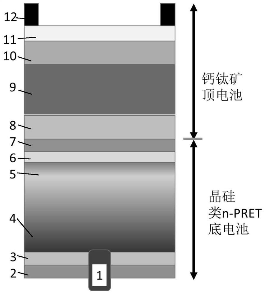
[0026] The perovskite / crystalline silicon tandem solar cell structure includes: a bottom cell and a perovskite top cell; the bottom cell is a crystalline silicon-PERC bottom cell; the perovskite top cell includes a perovskite cell current-carrying cell The sub-transport layer A8, the perovskite absorption layer 9, the perovskite battery carrier transport layer B10, the transparent conductive film 11 and the top electrode grid line 12; the top electrode grid line 12 is located on the top of the transparent conductive film 11;

[0027] The structure of the crystalline silicon-PERC bottom cell from bottom to top is back electrode gate line 1, passivation layer A2, passivation layer B3, p-type silicon wafer 13, n-type doped emitter 14, ultra-thin The tunneling dielectric layer 6 and the heavily doped polysilicide film 7; the back electrode gate line 1 is embedded in the passivation layer A2 and the passivation layer B3 and the bottom is in contact with the p-type silicon wafer 13; ...

Embodiment 2

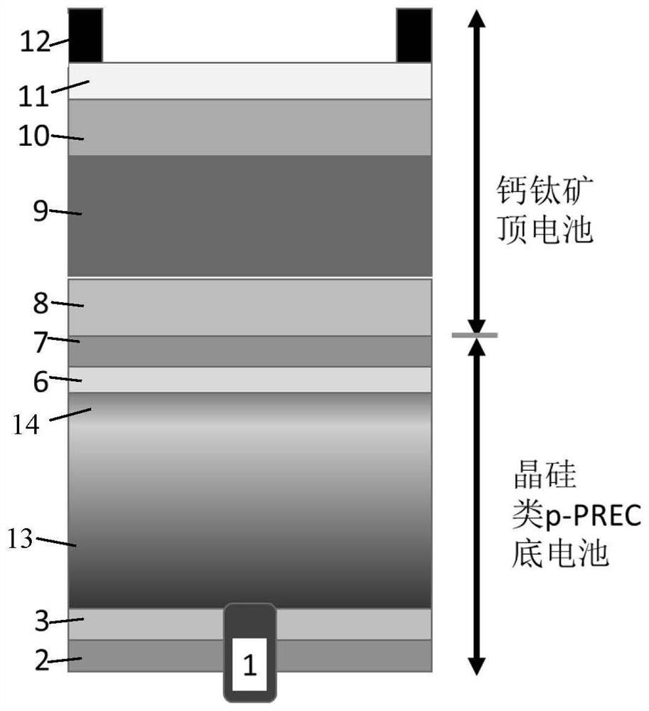
[0032] The perovskite / crystalline silicon tandem solar cell structure includes: a bottom cell and a perovskite top cell; the bottom cell is a crystalline silicon type-PERT bottom cell; the perovskite top cell includes a perovskite cell current-carrying cell The sub-transport layer A8, the perovskite absorption layer 9, the perovskite battery carrier transport layer B10, the transparent conductive film 11 and the top electrode grid line 12; the top electrode grid line 12 is located on the top of the transparent conductive film 11;

[0033] The structure of the crystalline silicon-PERT bottom cell from bottom to top is back electrode gate line 1, passivation layer A2, passivation layer B3, n-type silicon wafer 4, p-type doped emitter 5, ultra-thin The tunneling dielectric layer 6 and the heavily doped polysilicide film 7; the back electrode gate line 1 is embedded in the passivation layer A2 and the bottom of the passivation layer B3 in contact with the n-type silicon wafer 4; th...

Embodiment 3

[0039] The bottom cell is a planar n-PERT cell, the surface is prepared with silicon oxide, and the thickness of phosphorus-doped amorphous silicon is 20nm. After rapid annealing at 700°C for 10-300s, a tunnel junction is formed, and the contact resistivity is 10-20mΩ.cm2. The square resistance is 1000Ω / sq. On the tunnel junction, an electron transport layer with a thickness of 1-300 nm (which can be but not limited to TiO 2 , SnO 2 , ZnO, PCBM, C 60 , Nb 2 O 5 , SrTiO 3 , ICBA, ICTA and other materials), the thickness of 50 ~ 1500nm perovskite film (ABX 3 , where A is MA (methylamine), FA (formamidine), 5-AVA (5-ammonium isovalerate) or CS and their combination, B is Cu, Ni, Fe, Co, Mn, Cr, Cd, Sn , Pb, Pd, Ge, Eu or Yb and their combinations, X is I, Br or Cl and their combinations), a hole transport layer with a thickness of 1 to 300 nm (can be but not limited to spiro-OMeTAD, NiO x , CuI, CuSCN, NiO x , PEDOT: PSS, CuCSN, Graphene oxide, Cu 2 O, CuO, CuCaO 2 , P ...


PUM

PropertyMeasurementUnit
thicknessaaaaaaaaaa
thicknessaaaaaaaaaa
thicknessaaaaaaaaaa

Abstract

The invention relates to a perovskite / crystalline silicon stacked solar cell structure, comprising: a bottom cell and a perovskite top cell; the bottom cell is a crystalline silicon-PERC bottom cell or a crystalline silicon-PERT bottom cell; The perovskite top battery includes a perovskite battery carrier transport layer A, a perovskite absorption layer, a perovskite battery carrier transport layer B, a transparent conductive film and a top electrode grid line; the top electrode grid line on top of the transparent conductive film. The beneficial effect of the present invention is: this kind of perovskite / crystalline silicon-PREC or perovskite / crystalline silicon-PERT can utilize the production line of present crystalline silicon PREC or PERT solar cell, only need to do a small amount of improvement, can Prepare a good bottom cell, improve the efficiency of solar cells, and reduce the production cost of perovskite / crystalline silicon stacked cells; this structure can form reliable full-surface tunnel junction contacts without rectification effect; the preparation process is fully compatible with existing silicon The battery production method can be uniformly prepared on the whole surface, the process is simple, and the reliability is strong.

Description

technical field [0001] The invention relates to the field of solar cells, and particularly includes a perovskite / crystalline silicon stacked solar cell structure. Background technique [0002] In recent years, perovskite / crystalline silicon tandem solar cells have received extensive attention from the photovoltaic community. Since tandem cells can effectively utilize the solar spectrum, wide-bandgap perovskites absorb the short-wave part of sunlight to reduce hot electron losses, and crystalline silicon with narrow-band gaps absorbs long-wave parts to expand the spectral response of solar cells and reduce long-wave losses. The theoretical efficiency of double-junction solar cells is much higher than the theoretical limit of 29.4% for the efficiency of crystalline silicon single-junction solar cells. From the point of view of energy band matching, perovskite and crystalline silicon are ideal matching for double junction cells. As a new type of solar cell that has developed ...

Claims


Application Information

Patent Timeline
Patent Type & Authority Patents(China)
IPC IPC(8): H01L31/0725H01L31/0747H01L51/42
CPCH01L31/0747H01L31/0725H10K30/20Y02E10/549Y02P70/50
Inventor 寿春晖闫宝杰曾俞衡盛江叶继春丁莞尔郑晶茗
Owner ZHEJIANG ZHENENG TECHN RES INST
Why Eureka
Try Eureka