Diamond-based gallium nitride composite wafer and bonding preparation method thereof

A technology of diamond and gallium nitride, which is applied in the manufacture of microwave radio frequency devices and power electronic devices, the field of diamond-based gallium nitride composite wafer and its bonding preparation, and can solve wafer warpage, gallium nitride and diamond lattice constant Differences, difficulties in growing high-quality gallium nitride or diamond epitaxial layers, etc., to reduce pollution and shorten the time

Inactive Publication Date: 2020-11-06
XI AN JIAOTONG UNIV
View PDF18 Cites 6 Cited by
  • Summary
  • Abstract
  • Description
  • Claims
  • Application Information

AI Technical Summary

Problems solved by technology

For the first two methods, due to the large mismatch between the thermal expansion coefficients of GaN and diamond, epitaxial growth of diamond or GaN is carried out at a higher temperature, and there is a large stress in the e...

Method used


Image

  • Diamond-based gallium nitride composite wafer and bonding preparation method thereof
  • Diamond-based gallium nitride composite wafer and bonding preparation method thereof
  • Diamond-based gallium nitride composite wafer and bonding preparation method thereof

Examples


Embodiment 1

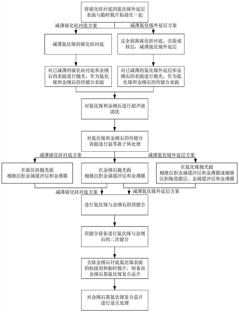
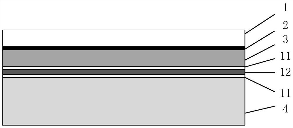
[0054] see figure 1 and figure 2 , the GaN-on-diamond composite wafer prepared by the present invention has the structure of GaN / nucleation layer / silicon carbide (5-80 microns) / metal buffer layer / gold film / metal buffer layer / diamond, and the specific preparation method includes the following step:

[0055] 1) bonding the surface of the gallium nitride epitaxial layer of the silicon carbide substrate gallium nitride to the silicon wafer (temporary carrier) with photoresist;

[0056] 2) The silicon carbide substrate is thinned to 40 microns by mechanical grinding;

[0057] 3) Carrying out surface polishing on the silicon carbide substrate and the diamond, so that the roughness of the polished surface of the silicon carbide substrate and the diamond is lower than 2 nanometers;

[0058] 4) Ultrasonic cleaning of gallium nitride and diamond with acetone, ethanol and deionized water successively;

[0059] 5) Put the gallium nitride and diamond into the sputter coater, use the p...

Embodiment 2

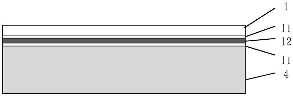
[0066] see figure 1 and image 3 The gallium nitride-on-diamond composite wafer prepared by the present invention has a structure of gallium nitride (1-3 microns) / metal buffer layer / gold film / metal buffer layer / diamond, and the specific preparation method includes the following steps:

[0067] 1) Using benzocyclobutene (BCB) to bond the surface of the gallium nitride epitaxial layer of the silicon carbide substrate gallium nitride to the silicon carbide wafer (temporary carrier);

[0068] 2) The silicon carbide substrate is thinned to 30 microns by mechanical grinding, and then the remaining silicon carbide substrate is etched away by inductively coupled plasma etching, the nucleation layer is removed, and the gallium nitride epitaxial layer is thinned to 2 microns;

[0069] 3) Surface polishing of the epitaxial layer of gallium nitride and diamond, so that the roughness of the polished surface of gallium nitride and diamond is lower than 2 nanometers;

[0070] 4) Ultrasoni...

Embodiment 3

[0078] see figure 1 and Figure 4 The gallium nitride-on-diamond composite wafer prepared in the present invention has a structure of gallium nitride (1-3 microns) / ceramic film layer / metal buffer layer / gold film / metal buffer layer / diamond, and the specific preparation method includes the following steps:

[0079] 1) Using 502 glue to bond the surface of the gallium nitride epitaxial layer of the silicon carbide substrate gallium nitride to the quartz plate (temporary carrier);

[0080] 2) The silicon carbide substrate is thinned to 50 microns by mechanical grinding, and then the remaining silicon carbide substrate is etched away by inductively coupled plasma etching, the nucleation layer is removed, and the gallium nitride epitaxial layer is thinned to 3 microns;

[0081] 3) Surface polishing of the epitaxial layer of gallium nitride and diamond, so that the roughness of the polished surface of gallium nitride and diamond is lower than 2 nanometers;

[0082] 4) Ultrasonic c...


PUM

PropertyMeasurementUnit
Thicknessaaaaaaaaaa
Thicknessaaaaaaaaaa
Thicknessaaaaaaaaaa

Abstract

The invention discloses a diamond-based gallium nitride composite wafer and a bonding preparation method thereof. The wafer is provided with a gallium nitride/nucleating layer/silicon carbide/metal intermediate layer/diamond substrate, a gallium nitride/metal intermediate layer/diamond substrate, a gallium nitride/ceramic film layer/metal intermediate layer/diamond substrate and other structures.The method mainly comprises the following steps of thinning a silicon carbide substrate of gallium nitride, or completely stripping the silicon carbide substrate and thinning a gallium nitride layer,carrying out polishing and argon plasma treatment on the silicon carbide substrate or the gallium nitride layer and the to-be-bonded surface of the diamond, depositing a metal buffer layer and a goldfilm on the to-be-bonded surface of the silicon carbide substrate, or depositing a metal buffer layer and a gold film on the to-be-bonded surface of the gallium nitride layer, or depositing a ceramicfilm layer, a metal buffer layer and a gold film, and depositing a metal buffer layer and a gold film on the to-be-bonded surface of the diamond, enabling gallium nitride and diamond to be pre-bondedat first, and then conducting secondary bonding, and carrying out annealing treatment on the diamond-based gallium nitride composite wafer. The bonding strength can be improved.

Description

technical field [0001] The invention belongs to the technical field of semiconductors and integrated circuits, and in particular relates to a diamond-based gallium nitride composite wafer and a bonding preparation method thereof, which can be applied to the manufacture of microwave radio frequency devices and power electronic devices. Background technique [0002] Gallium nitride is a third-generation semiconductor material. Compared with silicon and gallium arsenide materials, it has the characteristics of large band gap, high breakdown field strength, high saturation electron velocity, high temperature resistance and strong radiation resistance. It is very suitable for The production of high-temperature and high-power devices, high-frequency microwave devices, ultraviolet and nuclear radiation detection devices has extremely high application value in the technical fields of communication and power electronics. However, the serious self-heating effect and low thermal conduc...

Claims


Application Information

Patent Timeline
IPC IPC(8): H01L29/20H01L21/67
CPCH01L29/2003H01L21/67092
Inventor 胡文波白海洋王康吴胜利王宏兴曹梦逸谢荣华张宗民阮坤
Owner XI AN JIAOTONG UNIV
Why Eureka
Try Eureka