Passivating agent, passivating method thereof and method for preparing semiconductor film

A passivating agent, semiconductor technology, applied in the direction of semiconductor devices, semiconductor/solid-state device manufacturing, electric solid-state devices, etc., can solve the problems of battery hysteresis effect device performance deterioration, etc., to improve the quality, uniformity and repeatability of semiconductor film formation performance, improving stability

Pending Publication Date: 2020-12-15
HANGZHOU MICROQUANTA SEMICON CO LTD
View PDF5 Cites 8 Cited by
  • Summary
  • Abstract
  • Description
  • Claims
  • Application Information

AI Technical Summary

Problems solved by technology

[0003] Compared with other traditional solar cells, perovskite solar cells are more susceptible to moisture, oxygen, temperature, light and other factors, and perovskite solar cells are prone to ion migration under light, especially the migration of halogen ions. This phenomenon leads to the hysteresis effect of the battery and the deterioration of the device performance

Method used


Image

  • Passivating agent, passivating method thereof and method for preparing semiconductor film
  • Passivating agent, passivating method thereof and method for preparing semiconductor film
  • Passivating agent, passivating method thereof and method for preparing semiconductor film

Examples


Embodiment 1

[0069] Embodiment 1 of a preparation method of a perovskite layer solar cell of the present invention comprises the following steps:

[0070] (1) Clean the ITO transparent conductive glass, treat the surface with plasma, and set aside.

[0071] (2) CuI hole transport layer was prepared on ITO by slit coating method with a thickness of 30nm.

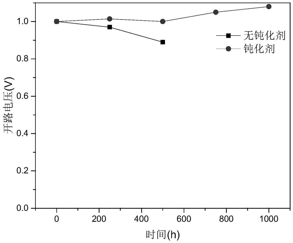
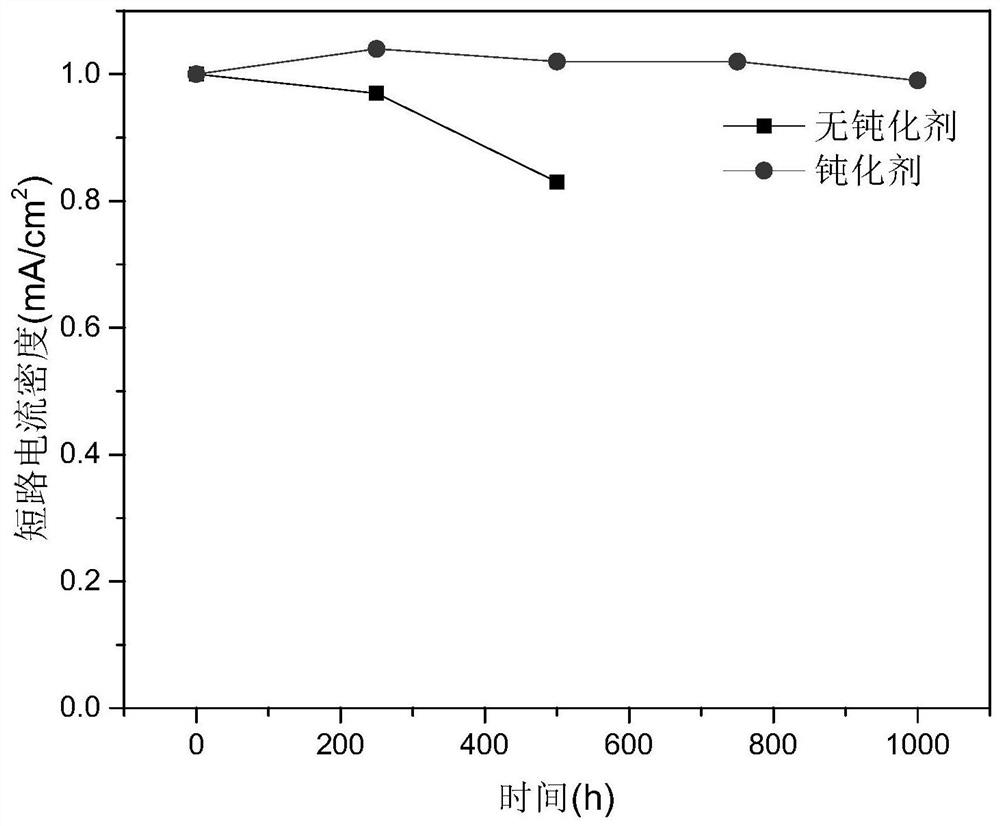
[0072] (3) Add the passivating agent—1-octyl-3-methylimidazolium bromide salt into methanol solvent to prepare a solution with a mass-volume ratio of 1 mg / mL. The solution was evenly coated on the surface of the hole transport layer material, and then baked at 100 degrees for 5 minutes.

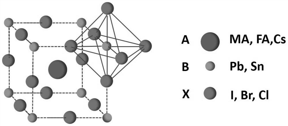
[0073] (4) Prepare the perovskite layer on the hole transport layer coated with passivating agent, adopt the co-evaporation method, and obtain the FAMACsPb(I) with a thickness of 500nm X Br 1-X ) 3 Perovskite thin film layer.

[0074] (5) The electron transport layer PCBM was prepared on the perovskite thin film layer, and a PCBM layer with a thickn...

Embodiment 2

[0077] Embodiment 2 of a preparation method of a perovskite layer solar cell of the present invention comprises the following steps:

[0078] (1) Clean the ITO transparent conductive glass, treat the surface with plasma, and set aside.

[0079] (2) CuI hole transport layer was prepared on ITO by slit coating method with a thickness of 30nm.

[0080] (3) The perovskite layer was prepared on the hole transport layer, and the co-evaporation method was used to obtain FAMACsPb(I) with a thickness of 500nm. X Br 1-X ) 3 Perovskite thin film layer.

[0081] (4) Add the passivating agent—1-octyl-3-methylimidazolium bromide salt into methanol solvent to prepare a solution with a mass-volume ratio of 1 mg / mL. The solution is evenly coated on the perovskite film layer, and then baked at 100 degrees for 5 minutes.

[0082] (5) The electron transport layer PCBM was prepared on the perovskite thin film layer, and a PCBM layer with a thickness of 10 nm was obtained by using a slit coati...

Embodiment 3

[0085] Embodiment 3 of a preparation method of a perovskite layer solar cell of the present invention comprises the following steps:

[0086] (1) Clean the ITO transparent conductive glass, treat the surface with plasma, and set aside.

[0087] (2) NiO hole transport layer was prepared on ITO by slot coating method with a thickness of 30nm.

[0088] (3) Add the passivating agent—1-hexyl-2,3-dimethylimidazolium tetrafluoroborate into the perovskite precursor solution PS, the molar ratio of the passivating agent to the total amount of halogen in the solution PS 1:1000, mix well.

[0089] (4) On the hole transport layer, the solution PS obtained in step (3) is used to prepare a perovskite layer, and the doctor blade coating method is used to obtain FAMACsPb(I X Br 1-X ) 3 Perovskite.

[0090] (5) The electron transport layer ZnO was prepared on the perovskite thin film layer, and a ZnO layer with a thickness of 100 nm was obtained by spraying.

[0091] (6) An electrode laye...


PUM

PropertyMeasurementUnit
thicknessaaaaaaaaaa
thicknessaaaaaaaaaa
thicknessaaaaaaaaaa

Abstract

The invention relates to a passivator. The ionic liquid comprises imidazolium salt ionic liquid, pyridinium salt ionic liquid, quaternary ammonium salt ionic liquid, quaternary phosphonium salt ionicliquid, pyrrolidine salt ionic liquid, piperidine salt ionic liquid, functionalized ionic liquid, ferrocene organic matter, a metal phthalocyanine compound, a metal acetylacetone compound and organicmetal, and at least one of a halogen bond compound and an organoboride. The invention also discloses a method for preparing a semiconductor film by using the passivating agent. The passivator is deposited between the semiconductor film and the interface material in contact with the semiconductor film and / or added into the raw material for preparing the semiconductor film, so a uniform and stable reaction environment is provided for the passivator and the semiconductor film material, and the crystal growth of the semiconductor film can be controlled in the preparation process; and stability ofthe semiconductor film is greatly improved.

Description

technical field [0001] The invention belongs to the technical field of semiconductor preparation, and in particular relates to a passivation agent, a passivation method and a method for preparing a semiconductor thin film. Background technique [0002] In recent years, a type of perovskite solar cell has received much attention. Perovskite as ABX 3 type of cubo-octahedral structure, such as figure 1 As shown, this perovskite solar cell uses organometallic halides as the light-absorbing layer. The thin film solar cell prepared by the material has the advantages of simple process, low production cost, stability and high conversion rate. Since 2009, the photoelectric conversion efficiency has increased from 3.8% to more than 22%, which is higher than the existing commercial crystalline silicon solar cells and has a greater cost advantage. [0003] Compared with other traditional solar cells, perovskite solar cells are more susceptible to moisture, oxygen, temperature, light...

Claims


Application Information

Patent Timeline
Patent Type & Authority Applications(China)
IPC IPC(8): H01L51/50
CPCH10K30/865H10K50/00
Inventor 不公告发明人
Owner HANGZHOU MICROQUANTA SEMICON CO LTD
Why Eureka
Try Eureka